RT5880 vs RT5870 vs RO3003 — Rogers PTFE PCB Material Comparison

Three Rogers PTFE materials cover the majority of RF and microwave PCB designs above 5GHz: RT5880 (Dk 2.20), RT5870 (Dk 2.33) and RO3003 (Dk 3.0). All three are PTFE ceramic composites requiring the same fabrication process — in-house plasma activation, controlled drill parameters and limited lamination cycles. But their different dielectric constants produce meaningfully different trace widths, insertion loss profiles and optimal applications. This guide explains when to choose each.

Table of Contents

Material Properties Comparison

PropertyRT5880RT5870RO3003RO4350B (ref)
Dk (10GHz)2.202.333.03.48
Df (10GHz)0.00090.00120.00100.0037
Insertion lossLowestVery lowLowModerate
Thermal conductivity0.20 W/m·K0.20 W/m·K0.50 W/m·K0.69 W/m·K
Process typePTFE — plasmaPTFE — plasmaPTFE — plasmaHydrocarbon
Thicknesses in stock6 (0.127–1.575mm)Available2 (0.127, 0.254mm)All standard
Prototype lead time7–10 days7–10 days7–10 days5–7 days

The Key Trade-off: Dk, Df and Trace Width

The three materials present a trade-off between two competing design priorities:

  • Lower Dk (RT5880 Dk 2.20) → wider 50Ω trace → lower insertion loss, but larger footprint
  • Higher Dk (RO3003 Dk 3.0) → narrower 50Ω trace → easier to route dense designs (77GHz arrays), but slightly higher loss

RT5870 (Dk 2.33) sits between the two — slightly narrower traces than RT5880 while maintaining very low Df (0.0012), making it useful for wideband designs where compact layout matters more than absolute minimum loss.

The difference in Df between RT5880 (0.0009) and RO3003 (0.0010) is small — approximately 10% — and for most applications within a single frequency band, RO3003 is chosen over RT5880 not because of Df but because of trace width: at 77GHz with 0.127mm substrate, the narrower 50Ω trace of RO3003 (~0.28mm) enables λ/2 patch spacing of ~1.95mm, which is not achievable with RT5880 (~0.34mm trace) in the same stack.

50Ω Trace Width ComparisonRogers RT5880 RT5870 RO3003 50 ohm microstrip trace width comparison chart showing wider traces for lower Dk materials
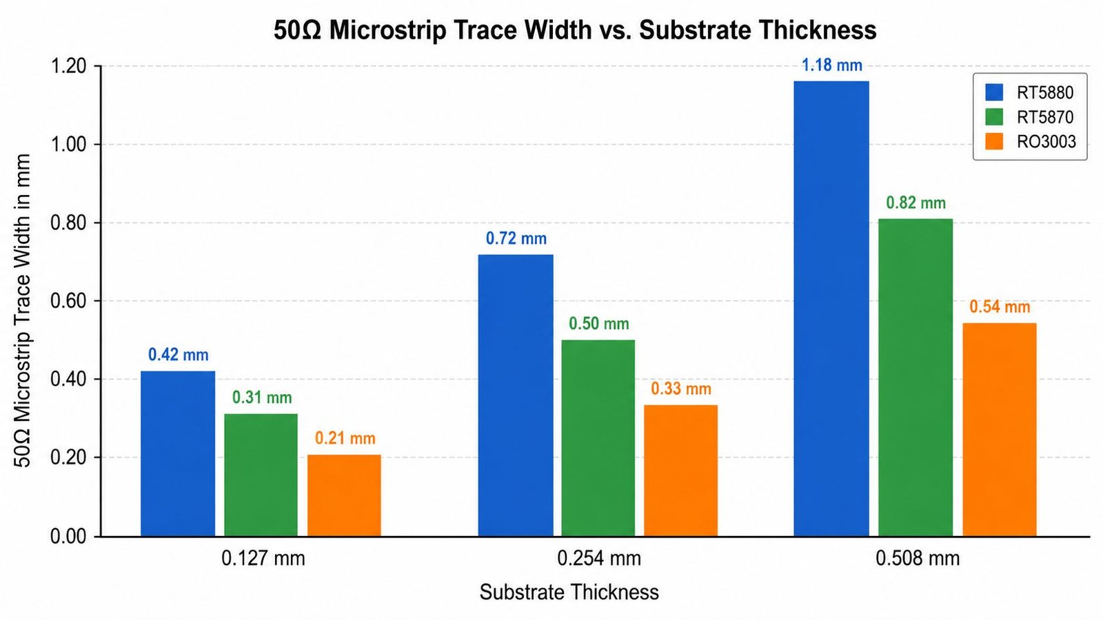
Substrate (thickness, copper)RT5880RT5870RO3003RO4350B
0.127mm, 0.5oz~0.34mm~0.30mm~0.28mm~0.26mm
0.254mm, 1oz~0.72mm~0.64mm~0.60mm~0.54mm
0.508mm, 1oz~1.42mm~1.28mm~0.95mm~0.83mm
0.787mm, 1oz~2.20mm~1.98mm~1.47mm~1.28mm

Trace widths are approximate and depend on production Dk tolerance. Always confirm 50Ω trace width against the actual material Dk certificate before tapering from design to production.

Application Selection Guide

ApplicationBest ChoiceReason
Wideband EW receiver 2–18GHzRT5880Lowest Df minimizes loss across wide BW
DRFM wideband inputRT5880Maximum loss budget preservation
77GHz FMCW radarRO3003 0.127mmLower Dk → narrower 50Ω trace → denser array
Ka-band patch antenna arrayRO3003 0.127mmDk ±0.04 uniformity critical for array pointing
Ka-band phased array (AESA)RO3003Tight Dk uniformity per panel
Compact wideband filterRT5870Slightly higher Dk → more compact vs RT5880
High power amplifier RF pathRO3003Higher thermal conductivity 0.50 W/m·K

When to choose RT5880

RT5880 is the primary choice when absolute minimum insertion loss is the design objective — wideband EW receivers, DRFM input stages, ESM/ELINT antenna feeds, and any design where the loss budget is tight across a wide instantaneous bandwidth. The wider trace width is a disadvantage for dense array designs but acceptable for most filter, amplifier and divider designs. RT5880 is available in 6 thicknesses in stock at Riching PCB — see Rogers RT5880 PCB manufacturer.

When to choose RT5870

RT5870 (Dk 2.33) provides a compromise between RT5880’s minimum loss and RO3003’s compact trace geometry. The slightly higher Dk produces traces approximately 10% narrower than RT5880 at the same thickness, useful when circuit density is a constraint but RO3003’s Dk 3.0 produces traces that are too narrow for the available etching tolerance.

When to choose RO3003

RO3003 (Dk 3.0) is the standard choice for 77GHz radar, Ka-band patch antenna arrays and Ka-band phased arrays where element spacing is constrained by the operating frequency. The narrower 50Ω trace width and tight Dk tolerance (±0.04) make it the correct material for designs where trace geometry precision and element-to-element consistency matter more than absolute minimum loss. RO3003 0.127mm and 0.254mm are in stock — see Rogers RO3003 PCB manufacturer.

Process Notes — All Three Materials

  • All three require in-house plasma activation — not outsourced — within 2 hours of copper plating
  • Maximum 2 lamination press cycles — enforced for all PTFE grades
  • PTFE-specific drill parameters — 40–60K RPM spindle speed
  • TDR impedance verification — ±10% standard, ±5% available on request
  • Rogers 2929 bondply available — for hybrid stackups combining any of these materials with FR4 inner layers

Frequently Asked Questions — RT5880 vs RT5870 vs RO3003

What is the difference between RT5880 and RO3003?
RT5880 (Dk 2.20, Df 0.0009) has lower dielectric constant and slightly lower loss than RO3003 (Dk 3.0, Df 0.0010). RT5880 produces wider 50Ω traces which limits its use in dense designs like 77GHz patch arrays. RO3003 is the standard for 77GHz radar and Ka-band arrays because its higher Dk produces narrower traces suitable for λ/2 element spacing at millimeter-wave frequencies.
When should I use RT5880 instead of RO3003?
Choose RT5880 when minimum insertion loss is the priority across a wide bandwidth — EW receivers, DRFM systems and wideband antenna feeds. RT5880 (Df 0.0009) has slightly lower loss than RO3003 (Df 0.0010), and the wider trace width is acceptable for most filter, amplifier and divider designs.
What is RT5870 used for?
RT5870 (Dk 2.33, Df 0.0012) provides a compromise between RT5880 and RO3003 — very low loss like RT5880, but slightly narrower traces. It is used in wideband designs where circuit density is a constraint but RO3003's trace width is too narrow for the available etching tolerance.
Do RT5880, RT5870 and RO3003 require the same manufacturing process?
Yes — all three are PTFE ceramic composites requiring in-house plasma activation within 2 hours of copper plating, PTFE-specific drill parameters and a maximum of 2 lamination press cycles. Factories without genuine in-house PTFE capability cannot reliably manufacture any of these materials.
PCB Project Review

Request a PCB Quote

Upload your Gerber ZIP file and project requirements. Our engineering team will review your PCB material, stackup, impedance needs, surface finish, and production quantity before quoting.

Please prepare:

  • Gerber files in ZIP format
  • PCB material or stackup requirements
  • Controlled impedance notes if available
  • Prototype or batch production quantity
ZIP format only. Please compress all Gerber and drill files into one ZIP package before uploading.