
UWB Positioning Module PCB Design — Antenna Keepout, RF/Digital Isolation & Clock Noise Control
UWB positioning modules for automotive digital keys, precise positioning, and industrial asset tracking run at 6-8GHz — far below 77GHz radar — but still need centimeter-level ranging accuracy. This guide covers antenna keepout zones, RF/digital isolation on a compact board, and crystal/power noise control for automotive and industrial UWB programs.
Home » UWB Positioning Module PCB Design for Automotive and Industrial Applications
Table of Contents
UWB Positioning Module PCB Design for Automotive and Industrial Applications: Antenna Keepout, RF/Digital Isolation, and Clock Noise Control
Ultra-wideband is moving well past digital car keys and asset tags. Combined UWB baseband-and-RF platforms now target automotive, industrial, and consumer applications at once, supporting non-line-of-sight ranging, anti-jamming performance, and UWB radar-style sensing under the IEEE 802.15.4ab standard. Industry forecasts put global UWB device shipments growing from roughly 597 million units to close to 1.18 billion units over the next several years, with automotive digital-key and precise-positioning use cases and industrial asset tracking as the two fastest-growing segments.
For a board house, that growth curve matters less than what it implies about the PCB itself: a UWB module is small, cost-sensitive, and produced in far higher volume than a radar or EW board — but it still has to hit centimeter-level ranging accuracy in the field. That accuracy depends on PCB-level details that are easy to get wrong on a board this size: antenna keepout, RF/digital isolation, and clock timing integrity.
Why a UWB Module Isn't Just "A Smaller RF Board"
UWB channels sit in the 6-8GHz range — for example, channel 5 near 6.5GHz and channel 9 near 8GHz — which is far below 77GHz automotive radar or 20-26GHz filter applications. Dielectric loss at these frequencies is comparatively forgiving, and that’s exactly why UWB module PCBs are often built on standard, cost-effective materials rather than specialty RF laminates.
What UWB does demand is timing precision. Ranging works by measuring time-of-flight with sub-nanosecond resolution, which means the antenna feed, the ground reference, and the reference clock all need to behave consistently from board to board and from unit to unit. A design that would be perfectly acceptable on a Wi-Fi or Bluetooth module can produce ranging error on a UWB module if the antenna environment isn’t controlled.
Antenna Keepout and Placement
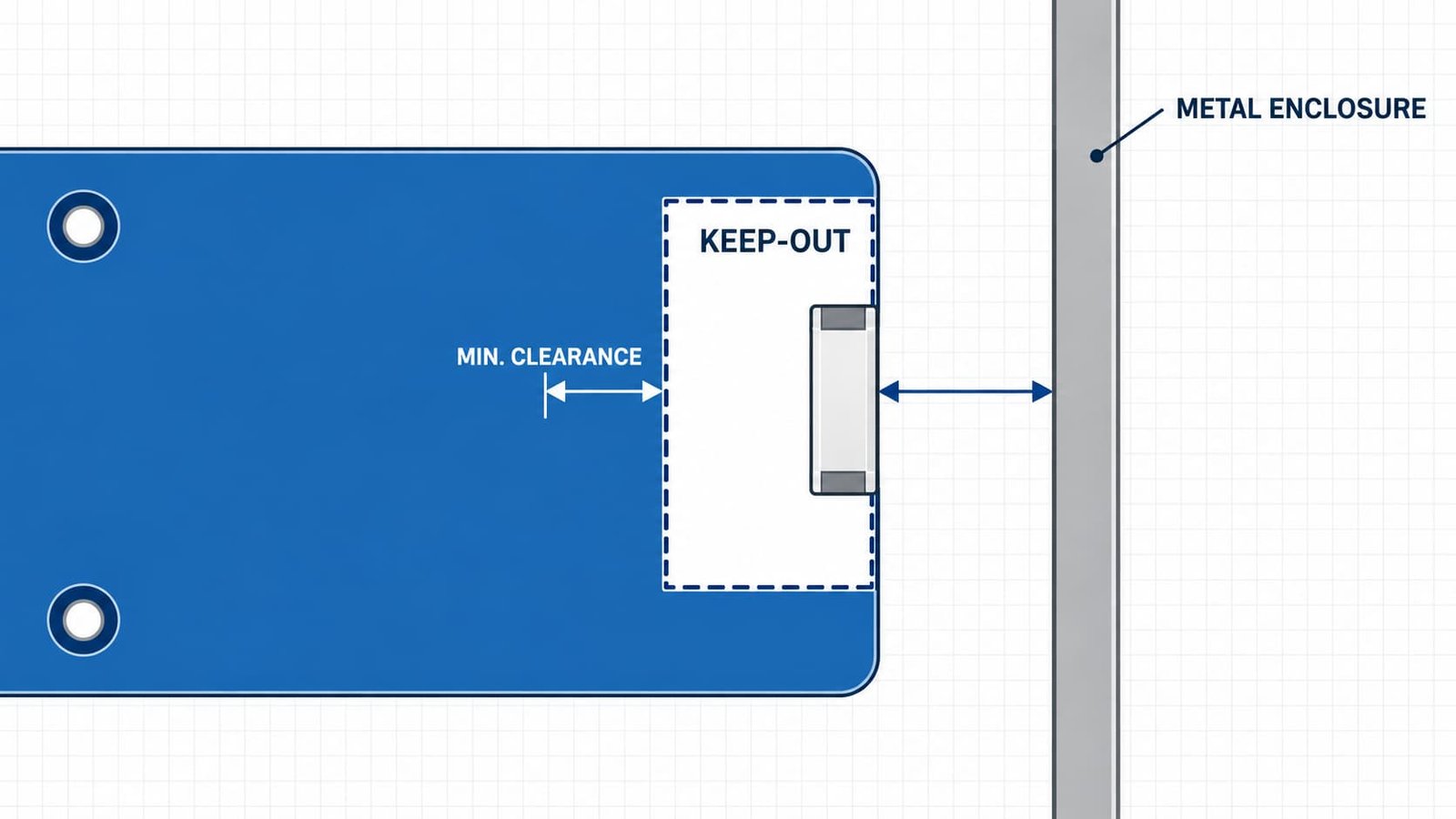
The antenna keepout zone is the single most common source of field-reported ranging problems on UWB modules. The area immediately around the antenna element — whether a chip antenna or a printed trace antenna — needs to be free of copper pours, ground fill, and component placement, and needs a defined minimum clearance to the nearest metal enclosure wall or battery pack. Skipping or shrinking this zone to save board space detunes the antenna and shifts its phase center, which feeds directly into ranging error even when the RF link budget still looks fine on paper.
Because the end product’s housing is rarely finalized when the PCB is designed, keepout dimensions should be validated against the worst-case enclosure the module is likely to sit inside, not just the reference design case.
| Zone / Element | Requirement | Typical Value | Notes |
|---|---|---|---|
| Antenna keepout zone | No copper pour, ground fill, or components around the antenna element | Per antenna vendor datasheet; validate against actual enclosure | Shrinking this zone detunes the antenna and shifts phase center |
| Antenna-to-enclosure clearance | Minimum air gap to nearest metal wall or battery pack | Per antenna vendor guidance; confirm with worst-case housing | Test across all enclosure variants the module may ship in |
| RF/digital ground fence | Stitching via row separating RF section from digital/host section | Tight pitch relative to 6-8GHz wavelength | Tie through to ground layer beneath the RF zone |
| Antenna feed line | Controlled 50Ω impedance, consistent panel-to-panel | ±10% or tighter, per design | Copper etch tolerance affects both loss and phase consistency |
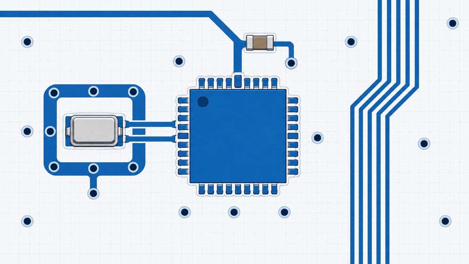
| Crystal oscillator footprint | Grounded guard ring; short, symmetric traces to IC | Trace length matched within a few mm | Keep digital/switching traces away from this area |
| RF/PLL power rail | Isolated or filtered supply, separate from digital host rail | Dedicated regulator or LC/ferrite filtering | Ripple on this rail modulates timing and phase |
| Digital host interface (SPI/I2C) | Routed away from RF near-field region | Cross RF traces at 90° only if unavoidable | Never run parallel to RF feed line for any length |
RF and Digital Isolation on a Small, Mixed-Signal Board
A UWB module packs an RF front end, a digital host interface (typically SPI or I2C to an application MCU), and power management onto a board that may only be a few square centimeters. The isolation principles are the same ones that apply to larger RF/digital boards — keep the RF section on its own reference plane, fence it with ground vias, and route digital traces away from the RF near-field region — but there’s less board area to work with, so the discipline has to be tighter, not looser.
The same fundamentals covered in our guide to RF and digital mixed-signal PCB stackup design apply directly here: a continuous ground reference under the RF section, a via fence around the antenna feed, and digital traces crossing the RF zone at right angles rather than running alongside it.
Crystal and Power Supply Noise Control
Ranging accuracy is a timing measurement, so the reference clock feeding the UWB IC is a direct contributor to error budget. Crystal oscillator layout should keep symmetric, short traces between the crystal and the IC, use a grounded guard ring around the crystal footprint, and avoid routing digital or switching power traces underneath or immediately alongside it. Power supply noise matters for the same reason: ripple or switching noise on the RF/PLL supply rail modulates timing and phase, so the RF section typically warrants its own regulator or filtering stage rather than sharing an unfiltered rail with the digital host interface.
Antenna keepout and clock-noise issues on a UWB module rarely show up on a bench S-parameter check — the RF link can measure fine while ranging accuracy is still off. These problems typically surface only during field or enclosure-level testing, by which point a board respin is a schedule and cost hit that a keepout review at the layout stage would have avoided.
Feed Line and Impedance Consistency
The trace from the UWB IC or module to the antenna needs controlled 50Ω impedance held consistently across production panels and board revisions, not just tuned once on a prototype. At 6-8GHz, copper etch tolerance and trace-width control have a measurable effect on feed-line impedance, which in turn affects both signal strength and the phase consistency that ranging accuracy depends on.
Material Notes
Standard FR-4 with tight process control is often sufficient for a UWB module’s operating band, which is one reason UWB hardware can scale to consumer and automotive volumes in a way that mmWave radar hardware can’t. Where a design also integrates a UWB radar-sensing function or shares the board with a higher-frequency radio, a mixed FR-4/low-loss laminate approach is worth evaluating on its own merits for that specific section of the board — the choice depends on which functions actually share the substrate, not a default upgrade.
Automotive vs. Industrial Quality Routes
Automotive UWB applications — digital key, precise positioning for keyless entry, in-cabin sensing — typically require IATF 16949 traceability and the batch-consistency discipline already familiar from automotive radar PCB programs, even though the UWB module itself sits at a much lower frequency and cost point. Industrial asset-tracking and positioning applications generally follow a different quality path, weighted more toward environmental robustness and long-term supply consistency than automotive-grade documentation. Knowing which route a given program needs before quoting materials and process controls avoids over- or under-building the quality system for the application.
What to Look for in a Manufacturing Partner
A UWB positioning module sits at a different point on the RF-board spectrum than a radar or EW board — smaller, higher volume, lower material cost — but it still needs specific capabilities most general-purpose board houses don’t carry as standard:
- Antenna keepout verification against the actual enclosure or housing design, not just the reference layout.
- RF/digital isolation practices scaled down correctly for a small, densely packed board.
- Controlled impedance repeatability panel-to-panel, not just on a single qualification build.
- The right quality system for the application — IATF 16949 traceability for automotive programs, or industrial-grade consistency for tracking and asset-management hardware.
UWB Positioning Module PCB Design — Q&A
Common questions on antenna keepout, RF/digital isolation, and clock noise control for UWB modules.
What frequency band does UWB positioning use, and does it need the same PCB treatment as mmWave radar?
UWB typically runs at 6-8GHz, far below 77GHz radar, so dielectric loss is less critical and standard FR-4 usually works. The real design focus is timing precision — antenna keepout, RF/digital isolation, and clock noise control — since ranging accuracy depends on phase and timing consistency, not just signal strength.
How much antenna keepout does a UWB module need?
It depends on the specific antenna and the nearest metal enclosure or battery, so there's no single number. The key is validating clearance against the actual worst-case housing the module ships inside, not just the reference layout — shrinking the zone detunes the antenna and shifts its phase center.
Why does crystal oscillator jitter affect UWB ranging accuracy?
UWB ranging measures time-of-flight at sub-nanosecond resolution, so the reference clock directly feeds into the error budget. Guard-ring grounding around the crystal and a clean, isolated RF/PLL power supply help keep that timing base stable.
Can the same PCB design serve both automotive and industrial UWB applications?
The RF and layout fundamentals carry over, but the quality system usually doesn't. Automotive programs typically need IATF 16949 traceability, while industrial tracking programs lean more on environmental robustness and supply consistency — worth confirming before quoting.
Building a UWB Positioning Module?
We build UWB positioning module PCBs for automotive digital-key and industrial tracking programs — with antenna keepout validation, RF/digital isolation, and the right quality system (IATF 16949 or industrial-grade) for your application.
Get a Quote → WhatsAppRequest a PCB Quote
Upload your Gerber ZIP file and project requirements. Our engineering team will review your PCB material, stackup, impedance needs, surface finish, and production quantity before quoting.
Please prepare:
- Gerber files in ZIP format
- PCB material or stackup requirements
- Controlled impedance notes if available
- Prototype or batch production quantity