
VCO/Oscillator PCB Design — Power Supply, Grounding, and Phase Noise
Low phase noise voltage-controlled oscillators, including surface-mount dielectric resonator types now shipping at 15GHz and similar frequencies, are only as clean as the board they sit on. This guide covers the PCB-level factors that determine whether an oscillator hits its rated phase noise in the field: power supply decoupling, tuning-voltage line cleanliness, ground return design, and the output transition into a 50Ω line.
Home » VCO/Oscillator PCB Design — Power Supply, Grounding, and Phase Noise
Table of Contents
Surface-mount dielectric resonator oscillators are reaching frequencies and phase-noise specifications that used to require larger, more expensive modules. A recent example running at 15GHz with 0-12V tuning, roughly 2MHz/V tuning sensitivity, and phase noise around -96dBc/Hz at a 10kHz offset is representative of where this class of device now sits — compact enough to place directly on a frequency synthesizer, local oscillator, or up/down-converter board.
That compactness is also the catch. A datasheet phase-noise number is measured on the vendor’s own evaluation board, under controlled power and grounding conditions. Move the same device onto a customer’s board with a noisier supply rail, a longer ground return, or a tuning line that picks up switching noise, and the measured phase noise can be meaningfully worse than the spec — through no fault of the device itself.
Why Phase Noise Is a PCB Problem, Not Just a Device Spec
An oscillator’s phase noise reflects how cleanly its output frequency holds steady over time, and two of the biggest external contributors to that stability are power supply ripple and tuning-voltage noise. Because a VCO’s frequency output is, by definition, a function of its tuning voltage, any noise riding on that line doesn’t just add background noise — it directly frequency-modulates the output. At a tuning sensitivity around 2MHz/V, even a small amount of ripple translates into a measurable phase-noise penalty, which is why the PCB around a VCO deserves the same scrutiny as the RF signal path itself.
Power Supply Decoupling and Isolation
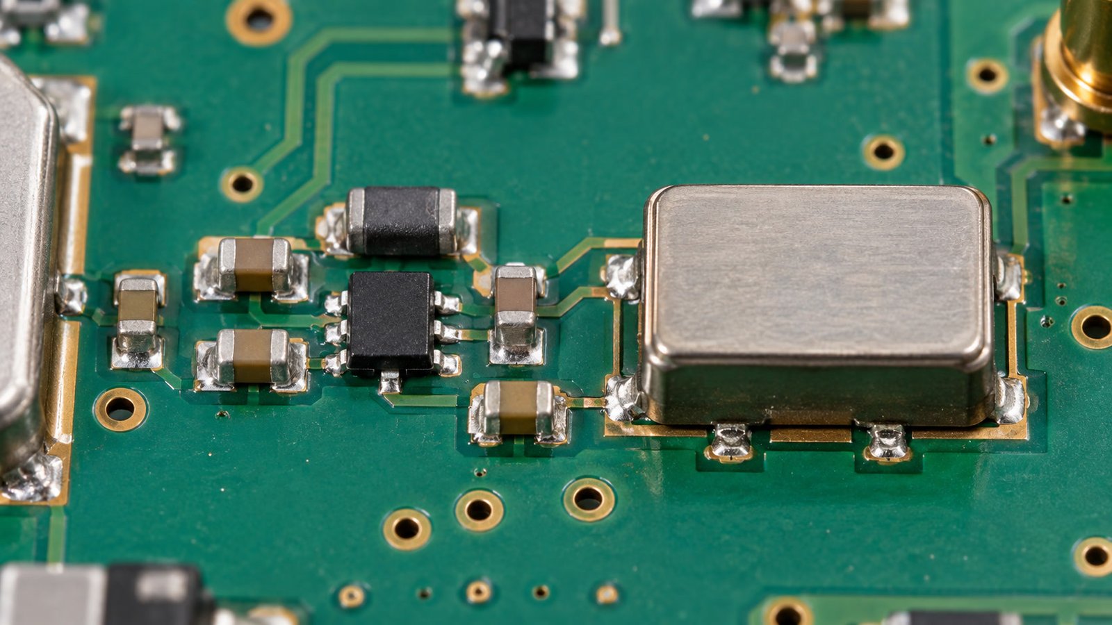
The oscillator’s DC supply rail should be decoupled directly at the device pins with a short, low-inductance path, and ideally isolated from noisier digital or switching-regulator rails elsewhere on the board through a dedicated linear regulator or an LC/ferrite filter stage. Sharing an unfiltered rail between a VCO and a digital section is one of the more common causes of phase-noise degradation that only shows up once the board is built and measured on a spectrum analyzer.
Tuning Voltage Line Cleanliness
The tuning voltage (Vtune) line deserves treatment closer to a sensitive analog signal than to a generic DC control line. It should be routed away from switching regulators, digital clocks, and any high-slew-rate signal, filtered at the point it enters the oscillator’s tuning pin, and referenced to a clean, low-noise ground rather than sharing a return path with noisier circuitry. Given the direct frequency-modulation relationship between tuning voltage and output frequency, this line has an outsized effect on measured phase noise relative to how little current it carries.
Ground Return and Shield Can Placement
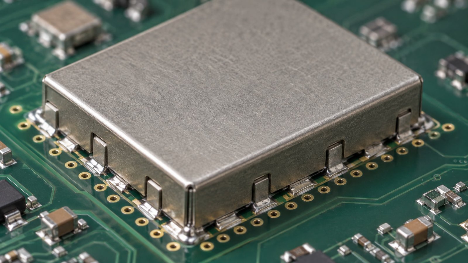
A VCO benefits from its own low-inductance ground reference, stitched with vias close to the package rather than relying on a long trace back to a shared ground point. Where a metal shield can is used — common on oscillator and synthesizer boards to control radiated emissions and isolate the VCO from nearby circuitry — consistent ground contact around the can’s entire perimeter matters as much as the ground plane underneath; a gap in that contact reintroduces the coupling the shield was meant to prevent. The same via-fencing discipline covered in our guide to RF and digital mixed-signal PCB stackup design applies directly to isolating an oscillator’s ground reference from the rest of the board.
Output Transition and 50Ω Continuity
The trace from the oscillator’s output pad to the board’s output connector needs a controlled 50Ω transition, typically microstrip or grounded coplanar waveguide depending on the stackup. A common design mistake at this stage is calculating trace width purely from a laminate’s nominal dielectric constant rather than from the actual bonded stack thickness and measured copper roughness of the fabricated board — the two can diverge enough at these frequencies to shift the finished impedance measurably away from 50Ω. Validating the transition against finished-board impedance testing, not just a calculated value, closes that gap.
| Parameter | Requirement | Why It Matters | Notes |
|---|---|---|---|
| Power supply decoupling | Short, low-inductance path at device pins | Ripple on the supply rail directly degrades phase noise | Common failure: shared unfiltered rail with digital section |
| Supply isolation | Dedicated regulator or LC/ferrite filter stage | Prevents digital/switching noise reaching the VCO | Especially important on synthesizer/converter boards |
| Tuning voltage (Vtune) line | Filtered, routed away from switching/digital signals | Directly frequency-modulates output (~2MHz/V typical) | Treat as sensitive analog, not a generic DC line |
| Ground reference | Low-inductance via stitching close to the package | Long return paths add noise coupling | Avoid sharing a long trace back to distant ground |
| Shield can grounding | Consistent contact around full perimeter | Gaps reintroduce the coupling the shield prevents | Check all sides, not just a few solder points |
| Output transition | 50Ω microstrip/CPW tuned to as-built stack | Nominal Dk can diverge from actual bonded thickness | Validate against finished-board impedance test |
| Material selection | Hydrocarbon-ceramic or PTFE per loss/cost/drift needs | Affects insertion loss and thermal frequency drift | Application-specific choice, not interchangeable |
Material and Stackup Notes
Hydrocarbon-ceramic RF laminates and PTFE-based materials both see use at 15GHz and similar frequencies for oscillator and synthesizer boards, with the choice depending on the specific balance of insertion loss, cost, and thermal drift the application needs — it’s an application-specific selection rather than a default substitution between the two families. Whichever material is chosen, designing the output transition from measured, as-built stack parameters rather than catalog Dk values is what actually determines whether the impedance lands where the design intended.
Phase-noise degradation caused by power supply ripple, a noisy tuning line, or an incomplete shield-can ground rarely shows up until the finished board is measured on a spectrum analyzer — by which point the fix usually means reworking the power and ground layout, not just re-tuning a matching network. Reviewing decoupling, tuning-line routing, and shield grounding at the layout stage is far cheaper than diagnosing a phase-noise shortfall after assembly. |
Where This Fits in a Larger RF System
A VCO or DRO board rarely stands alone — it typically feeds a frequency synthesizer, local oscillator chain, or up/down-converter module inside a larger radar, test, or communications system. The same grounding and material discipline covered in our radar and high-frequency PCB manufacturing guide and our Rogers/FR-4 hybrid stack-up guide carries over to the oscillator stage, just with tuning-line noise as an additional variable to control.
What to Look for in a Manufacturing Partner
A VCO or oscillator board rewards a few specific capabilities that aren’t always part of a general RF fabricator’s standard offering:
- Willingness to review power supply and tuning-line routing as part of DFM, not just check RF trace impedance.
- Consistent shield-can ground contact verified around the full perimeter, not just at a few solder points.
- Output transitions tuned from as-built stack measurements rather than nominal material Dk alone.
- Finished-board impedance and, where needed, phase-noise-relevant test data delivered alongside the boards.
VCO/Oscillator PCB Design — Q&A
Common questions on power supply, grounding, and phase noise for oscillator and synthesizer boards.
Why does power supply noise affect oscillator phase noise more than it affects typical digital circuits?
An oscillator's frequency depends directly on its supply and tuning conditions, so ripple modulates the output frequency itself rather than just adding noise. Digital circuits tolerate this far better since their output is a threshold decision, not a continuous frequency.
What makes the tuning voltage line different from other DC lines on a VCO board?
Tuning voltage sets the output frequency directly, often around 2MHz per volt of sensitivity. Noise on that line frequency-modulates the output, so it needs analog-grade filtering and routing care rather than generic DC-line treatment.
Why can't nominal Dk alone be used to design the output transmission line?
Catalog Dk is a nominal value - actual bonded thickness and copper roughness on a fabricated board can shift finished impedance measurably away from a calculated 50 ohms. Designing from as-built parameters and validating with impedance testing closes that gap.
Where should the shield can grounding be checked on an oscillator board?
Around the can's full perimeter, not just a few solder points. Any gap reintroduces the coupling the shield was meant to prevent, which can surface as elevated phase noise even when the RF circuit itself is designed correctly.
Building a Low Phase-Noise Oscillator Board?
We build VCO, DRO, and frequency-synthesizer PCBs with the power decoupling, tuning-line routing, and shield-can grounding discipline low phase-noise designs need.
Contact Us → WhatsAppRequest a PCB Quote
Upload your Gerber ZIP file and project requirements. Our engineering team will review your PCB material, stackup, impedance needs, surface finish, and production quantity before quoting.
Please prepare:
- Gerber files in ZIP format
- PCB material or stackup requirements
- Controlled impedance notes if available
- Prototype or batch production quantity