5G mmWave PCB: Material Selection, Design Rules and Manufacturing Guide

PCB substrate selection, stackup design and manufacturing requirements for 5G NR FR2 mmWave applications operating from 24 GHz to 40 GHz.

Table of Contents

Key point: Key point: Most factories quote 3–4 weeks waiting for RO3003 / RT5880 material procurement. Riching PCB maintains these materials in stock — no material wait.

Rogers RO3003 is a PTFE ceramic substrate with Dk 3.0 and Df 0.0010 — standard for Ka-band (26.5–40 GHz), 77 GHz automotive radar and 5G mmWave 28 GHz phased arrays. At 30 GHz, RO3003 insertion loss is ~0.5 dB/cm vs ~1.8 dB/cm for RO4350B. 50Ω microstrip on 0.127 mm RO3003 with 0.5 oz copper: ~0.28 mm trace width. Available thicknesses: 0.127 / 0.254 / 0.508 / 0.762 / 1.524 mm. All RO3003 orders require in-house plasma hole wall activation and maximum 2 lamination press cycles. Riching PCB stocks RO3003 in 0.127 mm and 0.254 mm with in-house plasma activation. No MOQ. Prototype 7–10 working days.5G mmWave PCB for FR2 bands (24–40 GHz) requires PTFE substrate — Rogers RO3003 (Dk 3.0, Df 0.0010) for 24–30 GHz, RT5880 (Dk 2.20, Df 0.0009) for 37–40 GHz. RO4350B (Df 0.0037) is suitable for FR1 sub-6GHz only. All PTFE materials require in-house plasma hole wall activation, low-profile copper foil, ENIG surface finish, and TDR impedance verification to ±5% on every production lot. Riching PCB stocks RO3003 and RT5880 with in-house plasma activation. No MOQ. Prototype lead time 7–10 working days.

5G mmWave PCB covers the 5G NR FR2 frequency range from 24.25 GHz to 40 GHz — the millimeter-wave bands that deliver multi-gigabit wireless speeds for fixed wireless access, dense urban coverage, and industrial private networks. At these frequencies, substrate material choice, copper foil type, and impedance control precision determine whether the antenna system meets its gain and beam-steering specifications or fails to meet range requirements.

This guide covers 5G FR2 frequency bands, material selection for each band, stackup design for mmWave antenna arrays, manufacturing requirements, and what to verify with your PCB fabricator.

5G FR2 mmWave Frequency Bands5G NR FR2 mmWave frequency bands table showing n257 n258 n260 n261 from 24 to 40 GHz

5G Band Frequency Region Recommended Material
n257 26.5–29.5 GHz USA, Japan, Korea RO3003 or RT5880
n258 24.25–27.5 GHz Europe, Asia RO3003 or RT5880
n260 37–40 GHz USA RT5880 or RO3003
n261 27.5–28.35 GHz USA RO3003 or RT5880
n262 47.2–48.2 GHz Global (planned) RT5880
FR1 sub-6GHz 410 MHz–7.125 GHz Global RO4350B or FR4 hybrid

The key distinction is between FR1 (sub-6GHz) and FR2 (mmWave). FR1 PCB can use Rogers RO4350B or even FR4 hybrid for lower frequencies. FR2 requires PTFE substrate across all bands from n257 through n261.

Why FR2 mmWave PCB Requires PTFE

At 28 GHz, the signal wavelength in RO4350B substrate is approximately 5.7 mm. Rogers RO4350B (Df 0.0037) produces insertion loss of approximately 2.5–3.5 dB/cm at 28 GHz. A typical 28 GHz antenna feed network spanning 8–10 cm introduces 20–35 dB of insertion loss — completely consuming the available link budget. PTFE substrates (RO3003, RT5880) with Df 0.0009–0.0010 reduce this to 0.6–1.2 dB/cm, preserving gain margin for the antenna array.

Dk stability over temperature is equally critical for mmWave antenna arrays. At 28 GHz, a ±0.05 variation in Dk shifts the patch antenna resonance by approximately 300–400 MHz — moving the element out of band and degrading array gain. Rogers RO3003 and RT5880 maintain Dk within ±0.05 from –40°C to +85°C.

Material Selection for 5G mmWave PCB

Material Dk Df Type 5G mmWave Suitability
RO3003 3.0 0.0010 PTFE ceramic ✅ Recommended — 24–30 GHz, stable Dk over temperature
RT5880 2.20 0.0009 PTFE glass ✅ Recommended — 37–40 GHz and wideband FR2
Taconic TLY-5 2.17 0.0009 PTFE glass ✅ Suitable — similar to RT5880
F4BM220 2.20 0.0010 PTFE ✅ Cost-effective — confirm Dk stability at 28 GHz
RO4350B 3.48 0.0037 Hydrocarbon ⚠️ FR1 sub-6GHz only — not suitable for FR2
Standard FR4 ~4.5 ~0.020 Epoxy glass ❌ Not suitable — excessive loss above 6 GHz

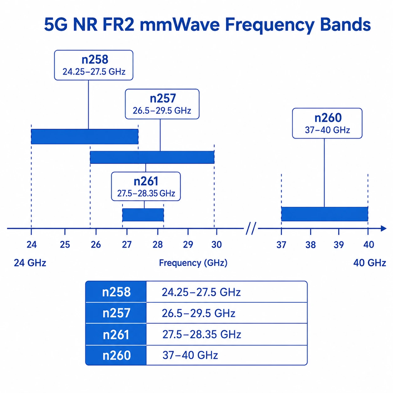
Rogers RO3003 (Dk 3.0, Df 0.0010) — Standard for 28 GHz

RO3003 is the most widely used substrate for 5G mmWave PCB at 24–30 GHz. Its Dk of 3.0 provides good trace width for manufacturing while Df 0.0010 keeps insertion loss within budget for antenna feed networks up to 10–12 cm. Available in 0.127 mm standard thickness for 28 GHz patch antenna designs.

Rogers RT5880 (Dk 2.20, Df 0.0009) — For 37–40 GHz and Wideband

RT5880 is preferred for 5G n260 band (37–40 GHz) where its lower Df provides better insertion loss performance, and for wideband designs spanning multiple FR2 bands. Its lower Dk produces larger antenna elements — antenna size must be recalculated when switching from RO3003 to RT5880.

RO4350B — Sub-6GHz FR1 Only

RO4350B (Df 0.0037) is suitable for 5G FR1 sub-6GHz applications (n77, n78, n79 bands up to 6 GHz) but is not suitable for FR2 mmWave. If your design includes both FR1 and FR2 antenna elements on the same board, a Rogers + FR4 hybrid stackup with RO3003 on outer RF layers and FR4 on inner layers is the standard approach.

Stackup Design for 5G mmWave Antenna PCB

2-Layer mmWave Antenna PCB (patch array)

  • Top copper: 0.5 oz (17 µm) finished — thin copper reduces surface roughness contribution
  • RO3003 core: 0.127 mm
  • Bottom copper: 1 oz (35 µm) finished — ground plane
  • Total board thickness: ~0.20 mm

For 50Ω microstrip on 0.127 mm RO3003 with 0.5 oz copper: trace width approximately 0.28 mm. For 0.254 mm RO3003: trace width approximately 0.60 mm. Always confirm with fabricator TDR before finalizing layout.

4-Layer Hybrid Stackup (mmWave + FR1 or digital)

  • L1 — RO3003 0.127 mm — mmWave RF signal layer
  • L2 — Ground plane
  • FR4 prepreg — power/signal distribution
  • L3 — Power plane or FR1 RF layer
  • FR4 prepreg
  • L4 — RO3003 0.127 mm — mmWave RF signal layer (bottom array)

This stackup supports dual-polarized antenna arrays or back-to-back antenna configurations. See FR4 + Rogers hybrid stackup guide for bondply selection and press cycle constraints.

Manufacturing Requirements

PTFE Plasma Activation

All 5G mmWave PCB substrates (RO3003, RT5880, Taconic, F4B) require in-house plasma hole wall activation before copper plating. Without this step, copper deposits on the PTFE hole wall with zero adhesion — boards pass initial electrical test and fail under thermal cycling from –40°C to +85°C cycling common in outdoor 5G base station equipment. See PTFE PCB manufacturing challenges for full process detail.

Copper Foil for mmWave

At 28 GHz, skin depth is approximately 0.38 µm. Standard electrodeposited (ED) copper foil surface roughness of 1–2 µm RMS significantly increases effective conductor loss. Low-profile (LP) or reverse-treated (RTF) copper foil with roughness below 0.5 µm RMS reduces insertion loss by 0.3–0.8 dB/cm at 28 GHz — a significant improvement for long antenna feed networks.

Impedance Control

5G mmWave PCB requires impedance control to ±5% or better, with TDR verification on every production lot. Trace width must be calculated using confirmed production Dk from the material certificate. For antenna-critical designs, request ±5% impedance tolerance explicitly on the fabrication drawing. See controlled impedance RF PCB guide for design rules.

Surface Finish

ENIG (immersion gold) is the standard surface finish for 5G mmWave PCB. The nickel layer (120–300 µin) provides a flat, consistent surface for microstrip impedance uniformity. HASL produces surface topology variation of 5–15 µm — unacceptable for 28 GHz patch antenna dimensions where element size tolerance is ±0.05 mm.

Applications5G mmWave massive MIMO antenna PCB array on Rogers substrate for base station application

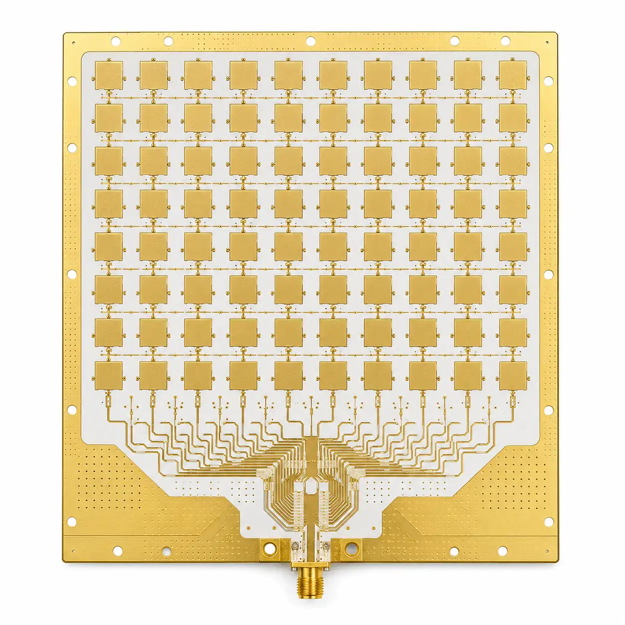
  • 5G NR FR2 base station massive MIMO antenna PCB — 64T64R and 32T32R arrays
  • 5G Fixed Wireless Access (FWA) CPE antenna module — indoor and outdoor units
  • 5G small cell antenna PCB — urban dense deployment
  • 5G mmWave test and measurement equipment — signal analyzers, vector network analyzers
  • Industrial private 5G network equipment — factory automation, robotics
  • 5G backhaul — point-to-point mmWave link antenna PCB

Conclusion

5G mmWave PCB for FR2 bands (24–40 GHz) requires PTFE substrate — Rogers RO3003 for most 28 GHz applications, RT5880 for 37–40 GHz and wideband designs. In-house plasma activation, low-profile copper foil, ENIG surface finish, and TDR impedance verification to ±5% on every production lot are non-negotiable requirements. Riching PCB manufactures 5G mmWave PCB with RO3003 and RT5880 in stock, in-house plasma activation, no MOQ, and prototype lead time of 7–10 working days. See high frequency PCB capabilities for full factory specifications.

Get a Quote for Your 5G mmWave PCB

Riching PCB stocks RO3003 and RT5880 with in-house plasma activation. Send the following for DFM review:

  • Gerber files + NC drill file
  • 5G band (n257 / n258 / n260 / n261) and operating frequency
  • Material grade and dielectric thickness
  • Stackup drawing — copper weight per layer
  • Controlled impedance target and tolerance
  • IPC Class and quantity

WhatsApp +86 13760473650 — DFM review within 24 hours

Q&A

5G mmWave PCB Q&A

Common questions about 5G mmWave PCB including FR2 material selection, difference from FR1, plasma activation, impedance requirements and prototype lead times.

What material is used for 5G mmWave PCB?

FR2 bands (24–40 GHz) require PTFE substrate. RO3003 (Dk 3.0, Df 0.0010) is standard for 24–30 GHz (n257, n258, n261). RT5880 (Dk 2.20, Df 0.0009) is preferred for 37–40 GHz (n260) and wideband designs. RO4350B is for FR1 sub-6GHz only — not suitable for FR2 mmWave.

What is the difference between FR1 and FR2 PCB material requirements?

FR1 sub-6GHz PCB can use RO4350B (Df 0.0037) or FR4 hybrid. FR2 mmWave (24.25–40 GHz) requires PTFE — RO3003 or RT5880 — with in-house plasma activation. Critical difference: RO4350B produces 2.5–3.5 dB/cm at 28 GHz versus 0.6–1.2 dB/cm for RO3003.

Why is in-house plasma activation important for 5G mmWave PCB?

5G base station equipment cycles from –40°C to +85°C outdoors. PTFE PCB without plasma activation has copper deposited with no adhesion — passes initial test, fails under thermal cycling. In-house plasma activation ensures consistent process control on every production lot.

What impedance tolerance is required for 5G mmWave PCB?

±5% or better, verified by TDR on every production lot. At 28 GHz, ±10% impedance causes significant antenna detuning and array gain degradation. Trace width must use confirmed production Dk from material certificate — not nominal datasheet values.

What is the prototype lead time for 5G mmWave PCB?

7–10 working days for RO3003 and RT5880 PTFE. No MOQ — from 1 board. DFM review before every order. WhatsApp: +86 13760473650.

PCB Project Review

Request a PCB Quote

Upload your Gerber ZIP file and project requirements. Our engineering team will review your PCB material, stackup, impedance needs, surface finish, and production quantity before quoting.

Please prepare:

  • Gerber files in ZIP format
  • PCB material or stackup requirements
  • Controlled impedance notes if available
  • Prototype or batch production quantity
ZIP format only. Please compress all Gerber and drill files into one ZIP package before uploading.