Electronic warfare (EW) systems are among the most demanding applications for high frequency PCB. Unlike radar systems that operate at a fixed frequency band, EW systems must detect, analyze, and respond to signals across extremely wide frequency ranges — often 2 GHz to 18 GHz or wider — with very high sensitivity, high dynamic range, and fast response time. The PCB inside an EW system carries broadband receive chains, high-power jamming amplifiers, frequency synthesis circuits, and digital signal processing interfaces, all with stringent isolation requirements between channels.
Rogers high frequency PCB materials — particularly Rogers RT5880 and RO3003 — are the standard choice for EW system PCB because they provide the combination of very low dielectric loss, stable and consistent Dk across a wide frequency range, and PTFE-base thermal stability that EW applications require. No other standard PCB laminate material matches this combination of properties across the 2–18 GHz EW frequency range.
This guide covers Rogers PCB material selection for EW systems, the electrical requirements that drive material choice, isolation and shielding design considerations, MIL-STD-461 EMC requirements, IPC Class 3 manufacturing standards, and what to prepare before production for EW system PCB.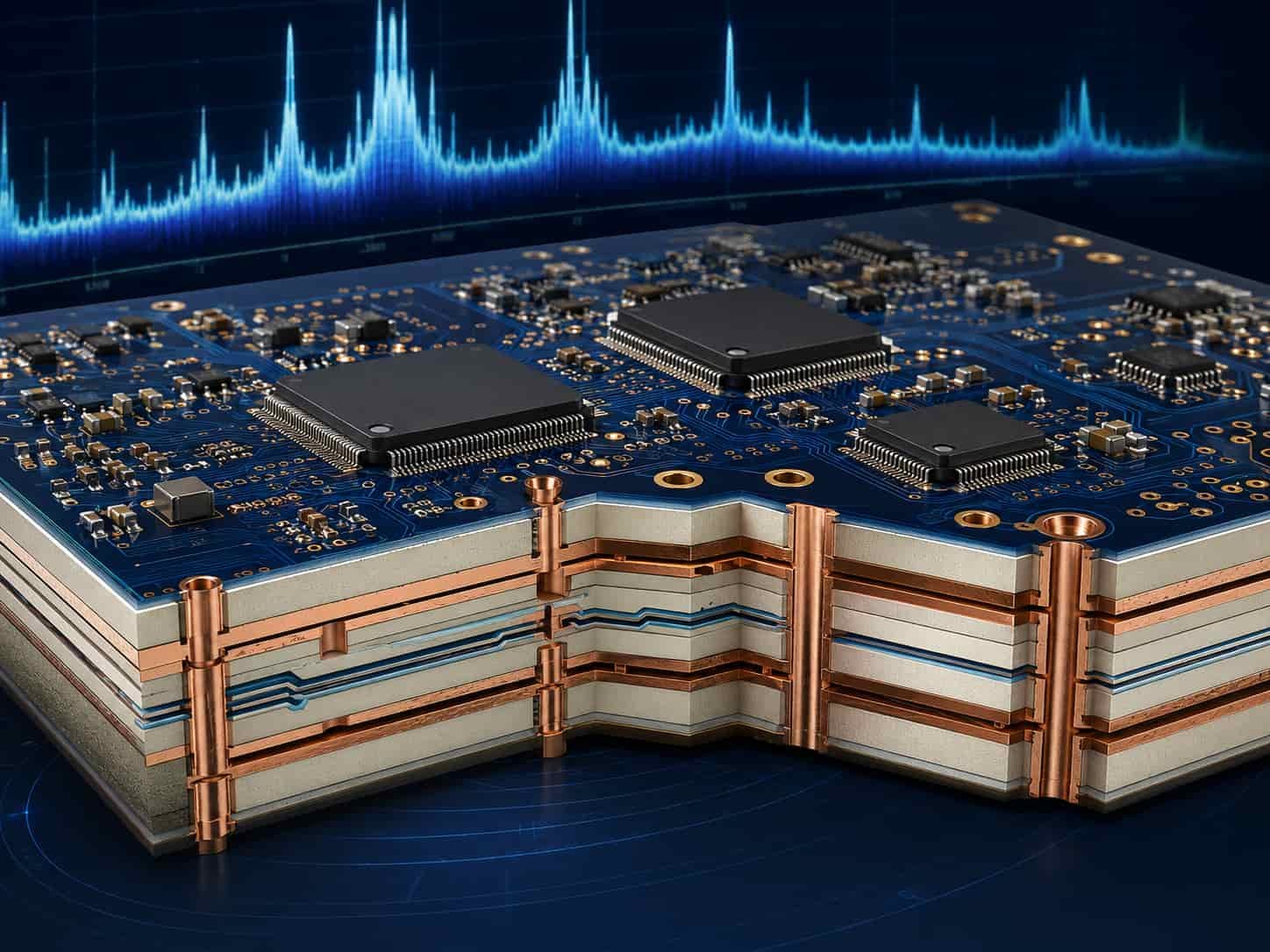
Quick Summary
Key point: Rogers RT5880 (Dk 2.2, Df 0.0009) is the primary material for wide-band EW PCB covering 2–18 GHz or wider. Rogers RO3003 (Dk 3.0, Df 0.0010) is used where slightly higher Dk is acceptable and CTE matching to copper is important. The key EW PCB requirements are stable Dk across wide frequency range, minimum insertion loss to preserve receiver sensitivity, high isolation between channels, thermal management for jamming amplifiers, and IPC Class 3 with MIL-STD-461 compliance.
The most important distinction between EW PCB and radar PCB is the bandwidth requirement. A radar operates at a defined frequency and can be optimized for that specific band. An EW system must work across an instantaneous bandwidth that may span a decade or more of frequency. Every tenth of a dB of insertion loss and every unit of Dk variation across this bandwidth affects system sensitivity and detection range.
Electronic Warfare System Types and PCB Requirements
Electronic warfare encompasses several system categories, each with different PCB design and material requirements. Understanding the system type is the starting point for correct Rogers PCB specification.
Electronic Support Measures (ESM)
ESM systems detect, intercept, identify, and locate electromagnetic emissions from radar, communication, and navigation systems. They are purely passive — receive only, no transmit. The PCB must support the lowest possible noise figure across the widest possible frequency range.
- Frequency coverage: typically 0.5–18 GHz, advanced systems to 40 GHz
- PCB requirement: minimum insertion loss from antenna to LNA — every dB of loss adds directly to noise figure
- Material: Rogers RT5880 — lowest Df of standard materials, minimum signal degradation across full band
- Channel isolation: very high — multiple simultaneous frequency band receivers must not interfere
- Dynamic range: very high — must detect weak signals in presence of strong emitters
Electronic Countermeasures (ECM) and Jamming
ECM systems transmit high-power RF signals to deny, degrade, or deceive enemy radar and communication systems. The PCB must handle significant RF power levels from GaN or GaAs power amplifiers while maintaining thermal stability and signal integrity in adjacent low-power receive circuits.
- Frequency coverage: matched to the threat frequency range — may be narrowband or wide-band
- PCB requirement: RF power handling, thermal management for PA chips, isolation between transmit and receive
- Material: Rogers RO3003 or RT5880 — CTE and thermal properties critical for PA chip reliability
- Thermal management: thermal via arrays under GaN PA packages — power density 5–20 W/mm²
- Switching: fast T/R switching to transition between jamming and receive modes
Radar Warning Receivers (RWR)
Radar warning receivers detect and identify radar emissions threatening the host platform. They must provide near-instantaneous threat detection across a wide frequency range with high probability of intercept. The PCB is purely receive-side but must achieve the combination of bandwidth, sensitivity, and response time that defines the system’s effectiveness.
- Frequency coverage: 2–18 GHz standard, advanced systems to 40 GHz
- PCB requirement: broadband antenna feed, low-loss LNA input circuit, fast switching between frequency bands
- Material: Rogers RT5880 — ultra-low Df preserves receive sensitivity across full RWR band
- Response time: PCB design must support fast scan rates — distributed receive architecture
- Size and weight: RWR PCB often highly miniaturized for airborne platform constraints
Directed Energy and Active Denial Systems
High-power directed energy systems use focused electromagnetic energy for non-kinetic effects. The PCB inside these systems handles the highest power levels in the EW spectrum and requires careful thermal management and power distribution design.
- Frequency range: system-dependent — microwave and millimeter-wave bands
- PCB requirement: very high power handling, thermal management, robust ground structure
- Material: Rogers RO3003 or RT5880 with thermal via arrays — thermal conductivity and power handling critical
Rogers PCB Material Selection for Electronic Warfare
The choice between Rogers RT5880 and RO3003 for EW PCB is driven by the specific combination of frequency range, insertion loss budget, CTE requirements, and power handling needs of the system.
Rogers RT5880 — Primary Choice for Wide-Band EW
Rogers RT5880 is the standard material for wide-band EW PCB covering the full 2–18 GHz or wider frequency range. Its combination of ultra-low Dk (2.2) and Df (0.0009), consistent Dk across frequency, and PTFE base thermal stability makes it the best performing standard PCB material for EW applications.
- Dk: 2.2 ±0.02 — lowest standard PCB material, maximum electrical wavelength on board
- Df: 0.0009 at 10 GHz — minimum dielectric loss across the EW frequency range
- Dk vs frequency: very stable from 1 GHz to 40 GHz — consistent electrical behavior across EW band
- Dk temperature coefficient: -125 ppm/°C — slight Dk decrease with temperature, must be included in design
- z-axis CTE: 237 ppm/°C — high, requires careful via design for thermal cycling reliability
- Available thicknesses: 0.127 mm to 3.175 mm — wide range supports different EW stackup requirements
- Applications: ESM broadband receivers, RWR systems, wide-band ECM, signal intelligence (SIGINT) receivers
Rogers RO3003 — For EW with CTE Priority
Rogers RO3003 is used in EW applications where CTE matching to copper is a priority — for example, large-aperture phased array EW systems or high-power ECM where via reliability under thermal cycling is more critical than achieving the absolute lowest Dk.
- Dk: 3.0 ±0.04 — higher than RT5880, shorter wavelength on board for same physical length
- Df: 0.0010 at 10 GHz — very low, adequate for most EW applications
- x-y CTE: 17 ppm/°C — closely matches copper, better via reliability in high thermal cycling applications
- z-axis CTE: 24 ppm/°C — much lower than RT5880, significantly better via fatigue life
- Applications: high-power ECM PCB with GaN PAs, large-aperture EW arrays, EW systems in extreme thermal cycling environments
Design guidance: For most airborne EW systems, Rogers RT5880 is the first choice because sensitivity across the full frequency band is the primary performance driver. For ground-based or ship-based EW systems where thermal cycling over long service life is the primary reliability concern, Rogers RO3003 offers better via fatigue life with acceptable insertion loss performance.
Wide-Band Electrical Performance Requirements for EW PCB
The most fundamental difference between EW PCB and narrowband radar PCB is the need for consistent electrical performance across a very wide instantaneous frequency range. Every electrical parameter — insertion loss, impedance, phase response — must be consistent from the low end to the high end of the EW operating band.
Insertion Loss Across the EW Band
Insertion loss in the PCB feed network adds directly to the EW system noise figure on receive and reduces effective radiated power on transmit. At microwave frequencies, dielectric loss (Df) dominates for most trace lengths encountered in EW PCB.
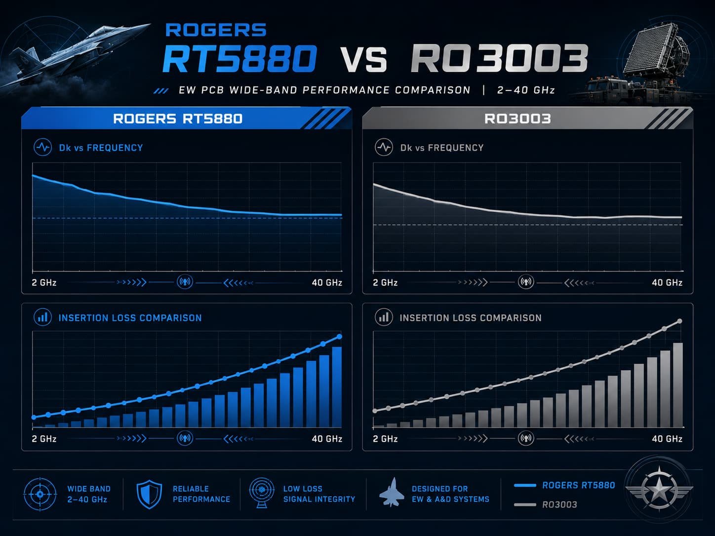
- Rogers RT5880 insertion loss: approximately 0.07 dB/inch at 10 GHz (50Ω microstrip, 0.508 mm substrate)
- Rogers RO3003 insertion loss: approximately 0.09 dB/inch at 10 GHz (same configuration)
- Standard FR4 insertion loss: approximately 0.5–0.8 dB/inch at 10 GHz — 6–10× higher than RT5880
- For a 6-inch feed network at 10 GHz: RT5880 adds ~0.4 dB loss, FR4 adds ~3–5 dB — difference equals noise figure degradation
- At 18 GHz, dielectric loss is approximately 1.8× the 10 GHz value — RT5880 advantage over FR4 increases
Dk Stability Across Frequency
As frequency increases, the Dk of most PCB materials decreases slightly. If Dk changes significantly from one end of the EW band to the other, the electrical length of transmission lines changes, which causes phase variation and impedance change across the band. This affects broadband matching, filter response, and antenna pattern.
- Rogers RT5880: Dk varies by approximately 0.02–0.03 from 1 GHz to 18 GHz — very stable
- Rogers RO3003: Dk varies by approximately 0.03–0.05 from 1 GHz to 18 GHz — stable
- Standard FR4: Dk varies by 0.3–0.5 from 1 GHz to 18 GHz — significant variation, unsuitable for EW
- Dk frequency stability must be confirmed from material data at the specific frequencies of interest
Impedance Control Across the EW Band
Controlled impedance in EW PCB must be maintained across the full operating frequency range. The impedance specification, tolerance, and coupon measurement frequency must all be defined to ensure the board performs correctly from the low end to the high end of the EW band.
- Standard impedance tolerance: ±10% for most EW PCB signal paths
- Broadband matching: trace width and ground plane geometry must be optimized for the full frequency range
- Impedance coupon: TDR measurement at production — confirms impedance at production frequency
- Broadband verification: simulation or measurement of insertion loss and return loss across full EW band
For controlled impedance background, see Why Controlled Impedance Matters in RF PCB Manufacturing.
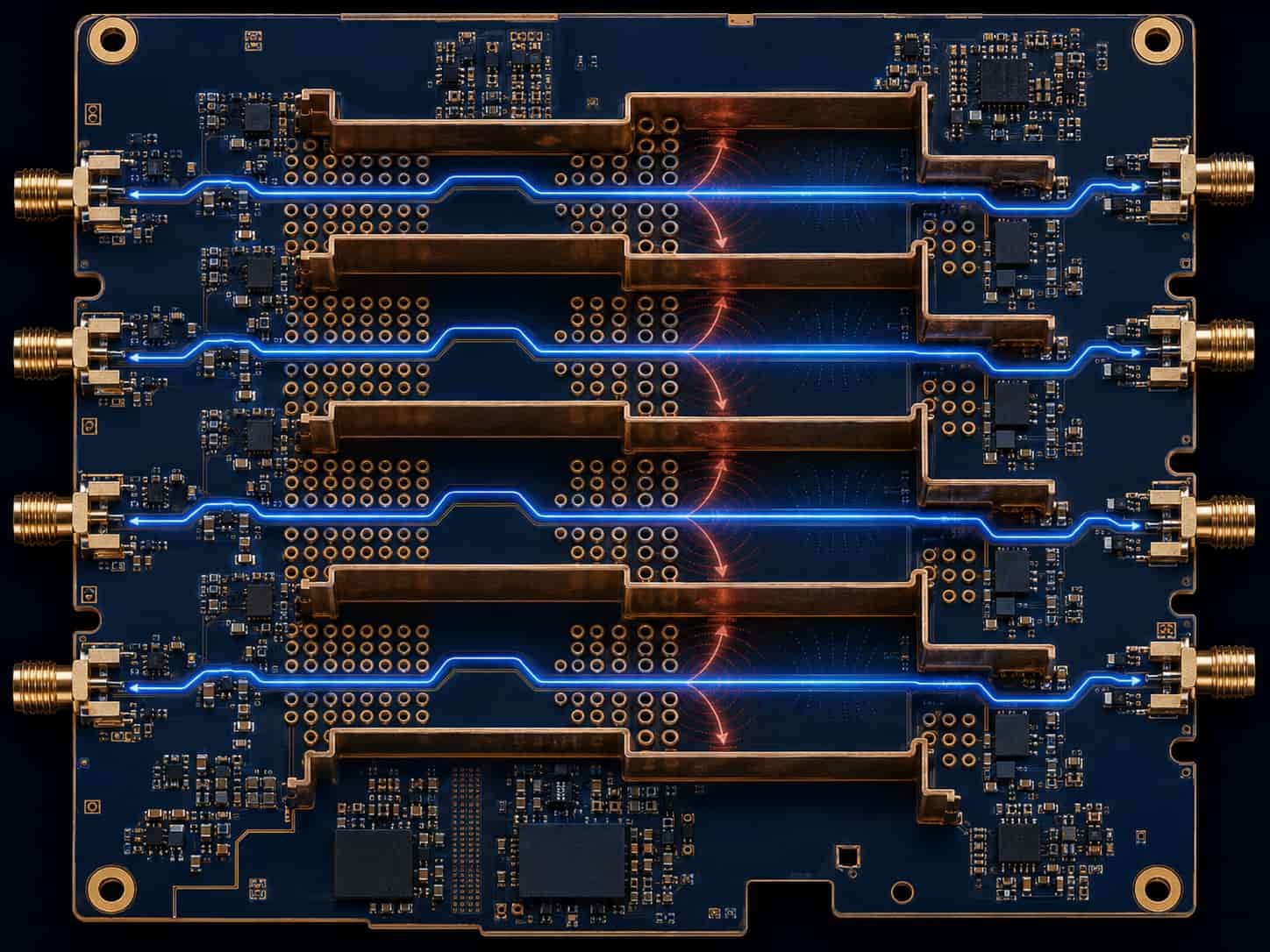
Isolation and Shielding Design in EW PCB
EW systems require extremely high isolation between receive channels, between transmit and receive paths, and between high-power and low-power circuits on the same board or in the same module. The PCB design plays a critical role in achieving the required isolation levels.
Via Fences for Channel Isolation
Via fences — rows of grounding vias placed along RF signal traces — are the most common PCB-level isolation technique in EW systems. They suppress lateral signal propagation in the substrate and reduce coupling between adjacent RF paths.
- Via fence spacing: typically ≤ λ/20 at the highest operating frequency to maintain shielding effectiveness
- At 18 GHz on Rogers RT5880 (Dk 2.2): λ/20 ≈ 0.57 mm — via pitch must be ≤ 0.57 mm
- Via diameter: 0.2–0.3 mm for dense EW via fences
- Via fences must be connected to the ground plane on every layer — not just the outer layer
- Isolation improvement: 20–40 dB additional isolation compared to no via fence
Metal Shielding Cans
For the highest isolation requirements in EW receivers — particularly where isolation between frequency bands must exceed 60–80 dB — metal shielding cans soldered to the PCB provide additional enclosure shielding beyond what via fences can achieve.
- Shielding can material: typically tin-plated steel or aluminum — soldered to continuous ground ring on PCB
- Ground ring: must be a continuous solderable pad with no gaps — via fence or solid ground fill underneath
- Can height: minimized to reduce parasitic resonance inside the cavity
- Feedthrough: signals passing through the can wall must use feedthrough capacitors or controlled-impedance apertures
Stripline vs Microstrip for EW Isolation
Stripline — a transmission line buried between two ground planes — provides inherently better isolation than surface microstrip because the signal is enclosed by ground copper on all sides. In EW receivers where isolation between receive channels is critical, stripline is often preferred over microstrip for the most sensitive signal paths.
- Microstrip: signal on outer layer, reference plane below — signal field partially in air above trace, some radiation
- Stripline: signal buried between two ground planes — fully enclosed, minimum radiation and coupling
- Stripline insertion loss: slightly higher than microstrip for same trace width due to two ground planes
- EW design practice: use stripline for sensitive receive paths, microstrip for antenna connections and output
MIL-STD-461 EMC Compliance for EW PCB
Military EW equipment must comply with MIL-STD-461 electromagnetic compatibility requirements. The PCB design directly affects radiated emissions, conducted emissions, and susceptibility performance that determine whether the equipment passes MIL-STD-461 testing.
Key MIL-STD-461 Requirements Affecting EW PCB
- CE102: conducted emissions on power leads — PCB power supply decoupling and filtering design
- RE102: radiated emissions from antenna terminals — spurious outputs from EW transmitters and synthesizers
- CS101: conducted susceptibility on power leads — PCB must reject power line noise
- RS103: radiated susceptibility — EW PCB must not malfunction under external RF illumination
- CS114: conducted susceptibility — cable bundle injection test affects PCB filtering requirements
PCB Design Practices for MIL-STD-461 Compliance
- Ground plane continuity: solid, unbroken ground planes minimize common-mode emissions and susceptibility
- Decoupling capacitors: placed as close as possible to power supply pins of all active components
- Filter boards: dedicated EMI filter boards at power entry points to equipment chassis
- Shielded enclosure: EW PCB typically housed in a fully shielded metal chassis — PCB ground must bond reliably to chassis
- Board-to-chassis ground: multiple low-impedance connections between PCB ground plane and chassis
- Connector filter: EMI filter connectors or filtered bulkhead connectors for signal and power entry
Note: MIL-STD-461 compliance is achieved at the equipment level, not the PCB level alone. The PCB design contributes to compliance through ground plane integrity, decoupling, and filtering, but the full EMI performance depends on the chassis, connectors, cables, and system-level shielding. Early EMC design review that includes PCB-level practices reduces the risk of failure during MIL-STD-461 testing.
Thermal Management in EW PCB
EW system PCB — particularly ECM and jamming systems — can have very high power density from GaN power amplifiers. Thermal management must be addressed at the PCB design level to ensure reliable chip junction temperatures across the operating temperature range.
- GaN jamming amplifier power density: 5–20 W/mm² at the chip level
- Thermal via array: 0.2–0.3 mm diameter, 0.5–0.7 mm pitch under GaN package
- Rogers RT5880 thermal conductivity: 0.20 W/m·K — relatively low, thermal vias essential
- Rogers RO3003 thermal conductivity: 0.50 W/m·K — 2.5× higher than RT5880 — better for high-power EW
- Copper coin insert: for GaN chips above 5W dissipation on RT5880 substrate — copper coin provides direct thermal path
- Heat spreader: PCB mounted to aluminum or copper heat spreader — PCB thermal resistance must be minimized
- Temperature rise budget: PCB thermal resistance must leave adequate margin for chip junction temperature
Multilayer Stackup Design for EW PCB
EW system PCB typically requires multiple layers to separate receive, transmit, local oscillator, digital, and power circuits while maintaining the required isolation between them.
- Typical EW PCB layer count: 8 to 20 layers for complex EW receivers and ECM systems
- Layer assignment: dedicate separate layers to receive RF, transmit RF, LO distribution, digital, and power
- Ground plane isolation: at minimum one ground plane between each RF signal layer
- Stripline layers: most sensitive receive circuits routed on buried stripline layers for maximum isolation
- PTFE material limitation: maximum 2 lamination cycles — limits blind via complexity in pure PTFE stackups
- Hybrid stackup: Rogers RT5880 on RF layers, high-speed FR4 on digital processing layers — reduces cost without sacrificing RF performance
For multilayer stackup design, see Multilayer High Frequency PCB: Layer Count, Stackup and Manufacturing Limits. For hybrid stackup options, see FR4 + Rogers Hybrid PCB Stackup: When Should You Use It?.
IPC Class 3 and Manufacturing Quality for EW PCB
EW system PCB requires IPC Class 3 workmanship. The combination of fine trace geometry, PTFE material processing, dense via fences, and high-power component assembly demands a manufacturer with demonstrated Class 3 capability for Rogers and PTFE materials.
- PTH copper plating: 25 µm average, 20 µm minimum — critical for EW PCB via reliability in thermal cycling
- No annular ring breakout: especially important for dense via fence structures
- 100% electrical test: continuity and isolation for every board
- PTFE hole wall activation: sodium or plasma etch before plating — essential for reliable via plating on RT5880
- Fine line capability: minimum 2.5 mil line width for dense via fence and RF trace structures
- Microsection FAI: verifies via plating thickness and dielectric integrity for Rogers PTFE boards
- Traceability: material certificates, laminate lot numbers, process records, board serialization
- MIL-PRF-31032: applicable for EW PCB required to meet US military PCB specifications
For IPC Class 3 details, see IPC Class 3 High Frequency PCB: What It Means for Aerospace and Defense Applications. For Rogers and PTFE manufacturing requirements, see High Frequency PCB for Aerospace and Defense: Material, Reliability and Manufacturing Requirements.
Information Needed for Electronic Warfare PCB Quotation
To review feasibility and provide an accurate quotation for EW system Rogers PCB, the following information should be prepared:
- Gerber files (all layers) and NC drill files
- Complete PCB stackup with material specification, layer sequence, and copper weight
- EW system type — ESM, ECM, RWR, SIGINT, or directed energy
- Operating frequency range — low and high end of EW band
- Material specification — Rogers RT5880, RO3003, or equivalent
- Layer count and board thickness
- Via structure — through-hole, blind, buried, via fence specifications
- Controlled impedance requirements — target, tolerance, frequency
- Thermal requirements — PA chip power dissipation, thermal via density
- IPC Class requirement — Class 3 for EW systems
- MIL-STD-461 applicability and test requirements
- Surface finish and thickness specification
- Traceability and documentation requirements
- Applicable standards — MIL-PRF-31032, MIL-STD-810, or other
- Quantity — prototype or production lot
For a complete file checklist, see What Files Are Needed for a High Frequency PCB Quotation?.

Conclusion
Rogers PCB for electronic warfare systems requires the combination of ultra-low dielectric loss, stable Dk across wide frequency ranges, and PTFE-base thermal stability that only Rogers RT5880 and RO3003 provide among standard PCB materials. Rogers RT5880 is the primary choice for wide-band EW receivers covering 2–18 GHz or wider. Rogers RO3003 offers better thermal cycling reliability for high-power ECM and large-aperture EW systems where via fatigue life is the critical reliability driver.
IPC Class 3 workmanship, PTFE-specific manufacturing processes, via fence design for channel isolation, thermal management for GaN amplifiers, and MIL-STD-461 EMC compliance are the framework within which high frequency PCB for electronic warfare must be designed and manufactured. Early engagement with a manufacturer experienced in Rogers and PTFE EW PCB reduces qualification risk and ensures the board meets the demanding combination of electrical, thermal, and reliability requirements that EW systems impose.