Most high frequency PCB projects for RF and microwave applications require more than two layers. Signal layers need dedicated reference planes for controlled impedance. Power and ground must be separated from RF signal routing. Shielding structures, via fences, and isolation between channels all require additional layers. As operating frequency increases and circuit density grows, the layer count requirement typically increases with it.
Multilayer high frequency PCB manufacturing combines the electrical requirements of RF PCB and microwave PCB design with the process complexity of multilayer lamination, controlled impedance verification, and tight layer registration. Material selection, stackup planning, lamination count, and via structure all affect the manufacturability and performance of the finished board.
This guide covers layer count options, minimum board thickness by layer count, stackup design considerations, impedance and registration tolerances, material constraints, and what information is needed before production.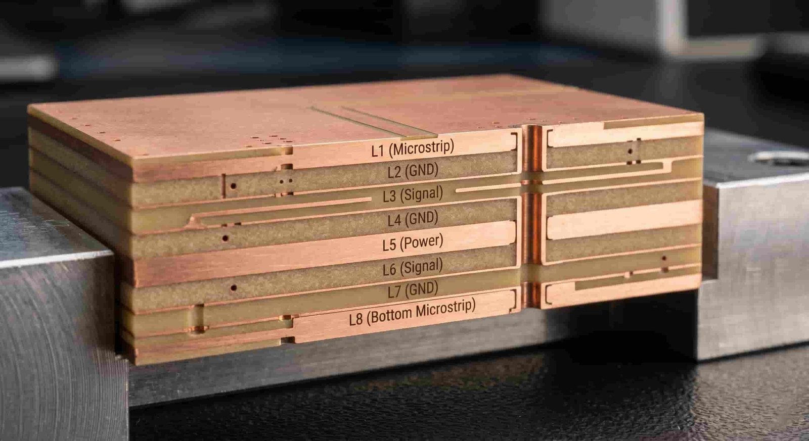
Quick Summary
Key point: Standard capability supports 1–32 layers. Advanced capability extends to 50 layers. Minimum board thickness increases with layer count: 0.2 mm for 2 layers, 0.36 mm for 4 layers, 0.575 mm for 6 layers. PTFE materials are limited to 2 lamination cycles. Layer registration tolerance is ≤ 0.1 mm standard and ≤ 0.05 mm advanced. Controlled impedance tolerance is ±10% standard and ±8% advanced for traces ≥ 50Ω.
Multilayer high frequency PCB requires stackup review before production. Layer count, dielectric material, dielectric thickness, copper weight, via structure, and impedance targets must all be confirmed together — changing one parameter affects the others.
Why High Frequency PCB Projects Require Multiple Layers
A single or double-sided board can support basic RF circuits at lower frequencies, but most practical RF and microwave designs require at least 4 layers. The reasons are structural and electrical:
Reference Plane for Controlled Impedance
Microstrip and stripline transmission lines both require a continuous copper reference plane at a controlled distance from the signal trace. In a 2-layer board, the reference plane is the opposite side of the board, which limits dielectric thickness control and makes impedance calculation less reliable. In a 4-layer or higher board, the reference plane can be placed immediately adjacent to the signal layer, allowing precise impedance control with thinner dielectrics.
Separation of RF Signal and Power
RF signal layers must be isolated from power supply noise. Placing power and ground on dedicated inner layers, separated from the RF signal layers by dielectric and reference planes, reduces power supply interference and improves signal integrity at high frequencies.
Shielding and Isolation
In multichannel RF designs — such as phased arrays, radar front-ends, or multi-band antenna systems — different RF signal paths must be isolated from each other. Additional ground layers between signal layers, combined with via fences, provide channel-to-channel isolation that would not be achievable on a 2-layer board.
Component Density
RF and microwave modules often have high component density with fine-pitch BGAs, QFN packages, and RF connectors on the same board. Multilayer routing allows signals to be distributed across layers, reducing trace congestion and minimizing RF coupling between adjacent traces.
For via design in multilayer RF boards, see Via Design Considerations for RF PCB Manufacturing. For blind via capabilities in multilayer designs, see Blind and Buried Via Capabilities in High Frequency PCB Manufacturing.
Layer Count and Minimum Board Thickness
The table below summarizes layer count options and minimum board thickness for high frequency PCB. Minimum thickness increases with layer count because each additional copper and dielectric layer adds to the total stackup height.
Layer Count | Min. Board Thickness | Standard Capability | Advanced Capability |
2 layers | 0.2 mm | ✓ | ✓ |
4 layers | 0.36 mm | ✓ | ✓ |
6 layers | 0.575 mm | ✓ | ✓ |
8 layers | 0.785 mm | ✓ | ✓ |
10–16 layers | ~1.0–2.0 mm | ✓ | ✓ |
18–32 layers | ~2.0–5.4 mm | ✓ | ✓ |
33–50 layers | Review required | – | ✓ (Engineering review) |
* Each additional 2 layers above 6 layers adds approximately 0.21 mm to the minimum board thickness. Boards above 9 mm require individual engineering review.
Design guidance: For most RF and microwave PCB projects, 4 to 16 layers cover the majority of designs. 4-layer boards suit compact RF modules and antenna boards with moderate complexity. 8 to 12 layers are common for radar front-ends, phased arrays, and multi-channel RF systems. Above 16 layers, detailed stackup review and engineering sign-off are recommended before production.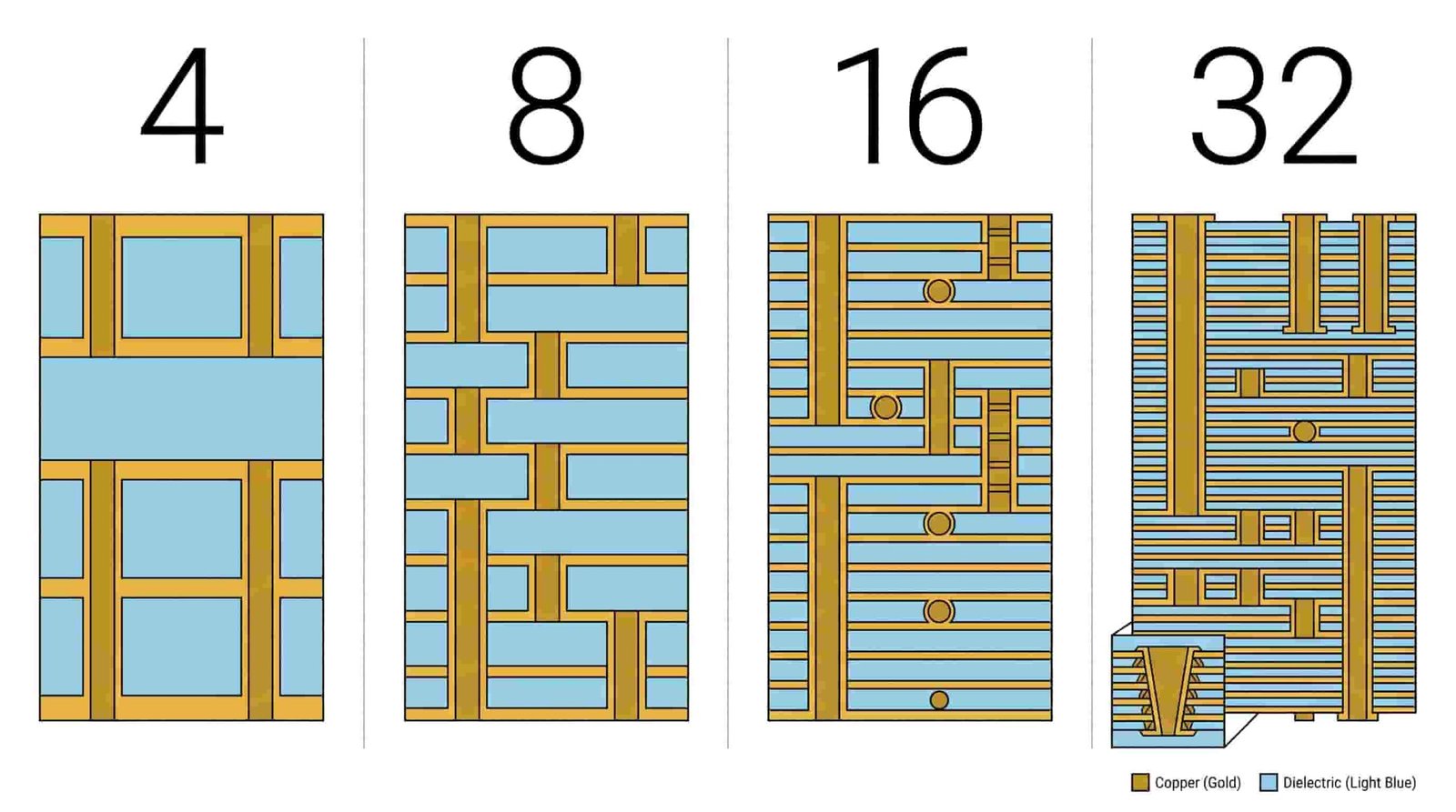
Multilayer Stackup Design for High Frequency PCB
Stackup design for multilayer high frequency PCB is more complex than for standard FR4 digital boards. Every layer assignment, dielectric material, and copper weight affects impedance, signal loss, crosstalk, and manufacturing feasibility.
Symmetrical Stackup
Multilayer high frequency PCB should use a symmetrical stackup — the layer sequence above the center of the board should mirror the sequence below. A symmetrical stackup minimizes warpage during lamination, which is especially important for PTFE-based materials that are more sensitive to thermal cycling than FR4.
- Copper balance across all layers prevents bow and twist after lamination
- Asymmetric stackups are more prone to warpage, especially in thin boards
- Warpage tolerance: ≤ 0.75% for SMT boards, ≤ 1.0% for through-hole component boards (standard); tighter in advanced capability
Microstrip vs Stripline Configuration
The choice between microstrip and stripline transmission line configuration affects the stackup assignment and the number of layers needed:
- Microstrip: signal trace on outer layer, reference plane on first inner layer. Easier to probe and measure. Slightly higher radiation loss at very high frequencies.
- Stripline: signal trace buried between two reference planes on inner layers. Lower radiation loss, better isolation. Requires more layers to implement.
- Buried microstrip: outer layer signal with reference plane on second inner layer, with ground fill on first inner layer. Hybrid approach used in some designs.
Ground and Power Plane Assignment
- Dedicate at least one full inner layer as a continuous ground reference plane adjacent to each RF signal layer
- Avoid splitting ground planes under RF traces — splits create impedance discontinuities
- Power planes should not be adjacent to RF signal layers without a ground plane between them
- In designs with mixed RF and digital layers, assign ground planes between RF and digital signal layers to reduce coupling
For detailed stackup planning guidance, see RF PCB Stackup Design: Key Factors Before Manufacturing.
Impedance and Layer Registration in Multilayer High Frequency PCB
Two of the most critical parameters in multilayer high frequency PCB manufacturing are controlled impedance tolerance and layer-to-layer registration accuracy. Both must be confirmed during stackup review.
Parameter | Standard | Advanced |
Impedance tolerance (< 50Ω) | ±5Ω | ±3.5Ω |
Impedance tolerance (≥ 50Ω) | ±10% | ±8% |
Layer registration tolerance | ≤ 0.1 mm | ≤ 0.05 mm |
Min. dielectric thickness (CORE+foil) | 0.065 mm (1080H) | 0.05 mm (106H) |
Warpage | ≤ 0.75% (SMT) | ≤ 0.5% (SMT) |
Max. board thickness | 5.4 mm | 12 mm |
Controlled Impedance in Multilayer Boards
In a multilayer board, impedance is affected by trace width, dielectric thickness, copper weight, and the distance to the reference plane. As layer count increases, the inner dielectric thicknesses become thinner and more difficult to control precisely. Each lamination cycle introduces slight variation in dielectric compression.
- Impedance coupons are placed on the panel edge to verify actual impedance after production
- Standard impedance tolerance is ±10% for traces ≥ 50Ω
- Advanced capability tightens this to ±8%
- For traces below 50Ω, absolute tolerance applies: ±5Ω standard, ±3.5Ω advanced
Layer Registration
Layer registration is the accuracy with which inner layers align to each other and to the outer layers after lamination. In multilayer high frequency PCB, poor registration affects via pad ring width, blind via placement accuracy, and layer-to-layer isolation.
- Standard layer registration tolerance: ≤ 0.1 mm
- Advanced layer registration tolerance: ≤ 0.05 mm
- Tighter registration is required for fine-pitch via structures, HDI designs, and boards with small annular rings
For related information on layer registration and via design, see Drilling Capabilities for High Frequency PCB: Minimum Hole Size, Aspect Ratio and Tolerances.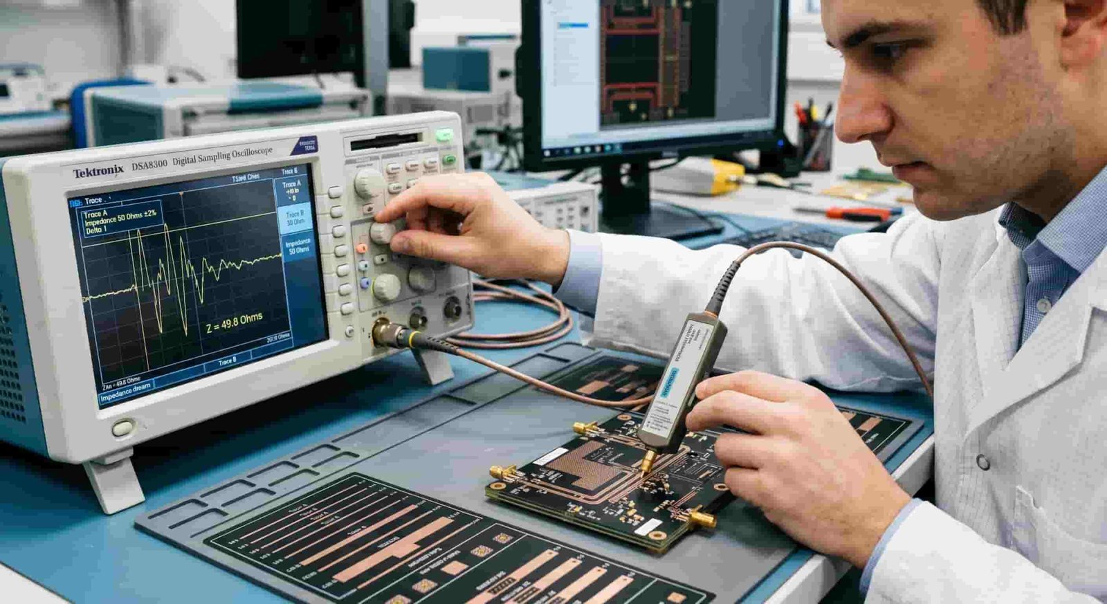
Material Options for Multilayer High Frequency PCB
Material selection for multilayer high frequency PCB must consider not just electrical performance but also lamination compatibility, thermal stability, and the number of press cycles the material can withstand.
Rogers Hydrocarbon Ceramic Materials (RO4000 Series)
Rogers RO4350B and RO4003C are the most widely used materials for multilayer RF and microwave PCB. They offer stable Dk, low Df, and compatibility with standard FR4 lamination processes, making them suitable for multilayer constructions with multiple press cycles.
- RO4350B: Dk 3.48, Df 0.0037 — balanced performance for most RF and microwave multilayer designs
- RO4003C: Dk 3.38, Df 0.0027 — lower loss, suitable for higher frequency multilayer boards
- Compatible with standard multilayer lamination equipment
- Supports up to 3 lamination cycles
Rogers PTFE Materials (RT/duroid Series)
Rogers RT5880 and RO3003 are PTFE-based materials used for multilayer high frequency PCB requiring very low loss. They have more demanding process requirements than hydrocarbon ceramic materials.
- RT5880: Dk 2.2, Df 0.0009 — ultra-low loss for millimeter-wave multilayer designs
- RO3003: Dk 3.0, Df 0.0010 — low loss, commonly used in radar and satellite communication multilayer boards
- PTFE materials limited to maximum 2 lamination cycles
- Require special surface preparation and bonding film for multilayer lamination
Taconic and F4B PTFE Materials
Taconic TLY-5, RF-35, and F4B series materials are alternative PTFE laminates used in multilayer high frequency PCB. They follow the same 2-cycle lamination limit as Rogers PTFE materials.
For detailed material properties and selection guidance, see Rogers PCB Material Selection Guide for RF and Microwave Applications, Taconic PCB Materials for RF and Microwave Applications, and F4B PCB Material Guide.
Hybrid FR4 + Rogers Multilayer Stackup
For cost-sensitive multilayer designs, a hybrid stackup using Rogers or PTFE material only on the RF signal layers and FR4 on the remaining layers is a common approach. This reduces material cost while maintaining RF performance on the critical layers.
- Rogers or PTFE on outer RF signal layers, FR4 on inner digital or power layers
- Bonding film compatibility between Rogers and FR4 must be confirmed
- CTE mismatch between materials must be reviewed for thermal reliability
- Lamination sequence and press parameters must account for both materials
For hybrid stackup design and manufacturing considerations, see FR4 + Rogers Hybrid PCB Stackup: When Should You Use It?.
Lamination Count and Its Effect on Layer Count
In multilayer PCB manufacturing, the board is built up through sequential lamination cycles. Each cycle presses and bonds a set of layers together. The maximum number of lamination cycles depends on the material type and limits the complexity of the via structure.
- FR4 and Rogers hydrocarbon ceramic: maximum 3 lamination cycles
- PTFE-based materials (Rogers RT/duroid, Taconic, F4B): maximum 2 lamination cycles
- Each blind or buried via stage requires one additional lamination cycle
- Through-hole only designs use fewer lamination cycles regardless of layer count
For high layer count boards with blind and buried vias in PTFE-based materials, the combination of layer count and via complexity must be reviewed carefully to confirm it is achievable within the lamination cycle limit.
For more on lamination cycle limits and blind via interaction, see Blind and Buried Via Capabilities in High Frequency PCB Manufacturing.
Surface Finish for Multilayer High Frequency PCB
Surface finish selection for multilayer high frequency PCB affects RF pad performance, solderability, and long-term reliability. The most common options for RF and microwave multilayer boards are:
- ENIG (Electroless Nickel Immersion Gold): standard choice for most RF multilayer boards. Flat surface, good solderability, compatible with controlled impedance design.
- ENEPIG (Electroless Nickel Electroless Palladium Immersion Gold): better for wire bonding and high-reliability RF pads. Nickel 120–300 µin, palladium 1–2 µin, gold 1–5 µin.
- Immersion Silver: very flat surface, low contact resistance, good for high frequency pads. Must be assembled quickly after surface finish due to tarnish sensitivity.
- OSP (Organic Solderability Preservative): lowest cost, suitable for simple RF boards without demanding pad requirements.
For detailed surface finish comparison for RF and microwave PCB, see Surface Finish Options for RF and Microwave PCB.
Information Needed for Multilayer High Frequency PCB Quotation
To review multilayer feasibility and provide an accurate quotation, the following information should be prepared:
- Gerber files (all layers including inner layers, solder mask, and silkscreen)
- Complete PCB stackup with layer sequence, dielectric material, dielectric thickness, and copper weight on each layer
- Layer count
- Total board thickness
- Via structure — through-hole only, blind, buried, or combination
- Material type — Rogers, PTFE, Taconic, F4B, FR4 hybrid, or other
- Controlled impedance requirements with target values, tolerance, and reference layer
- Surface finish
- Quantity — prototype or batch
- Working frequency range or application background
- Any special requirements — warpage tolerance, thermal management, IPC class
For a complete quotation checklist, see What Files Are Needed for a High Frequency PCB Quotation?.
Conclusion
Multilayer high frequency PCB manufacturing supports layer counts from 2 to 50 layers, with standard capability up to 32 layers and advanced capability beyond. Minimum board thickness, lamination count limits, layer registration tolerance, and controlled impedance specifications must all be confirmed during stackup review before production.
Material selection — whether Rogers PCB, PTFE PCB, Taconic, F4B, or hybrid FR4 + Rogers — affects lamination count limits, dielectric options, and via structure feasibility. A complete stackup with all layer parameters submitted before production reduces the risk of design changes, improves impedance consistency, and supports reliable prototype and batch results.