Controlled impedance is the most important manufacturing specification for RF and high-speed PCB. When a signal travels through a PCB trace, any mismatch between the trace impedance and the source or load impedance causes a reflection — signal power bounces back toward the source instead of reaching the destination. For RF circuits, impedance mismatch directly degrades performance: a 10% impedance deviation on a 50Ω trace produces a return loss of approximately -26 dB, which may be acceptable. A 20% deviation produces approximately -14 dB return loss — significant for most RF applications.
As a direct high frequency PCB factory, we verify controlled impedance with TDR on every production lot for all Rogers and PTFE boards. This guide covers everything engineers need to know to correctly specify, calculate, and verify controlled impedance PCB.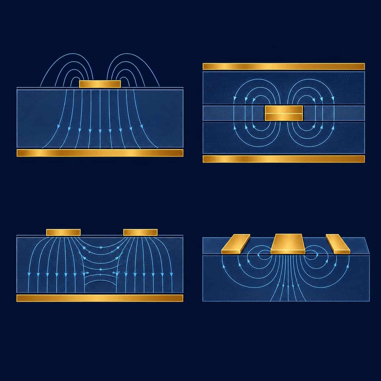
Quick Summary
Key point: Controlled impedance PCB requires: specifying the target impedance value (typically 50Ω single-ended or 100Ω differential), the tolerance (±10% standard, ±8% advanced), which layer carries the controlled trace, and the transmission line structure (microstrip, stripline, or coplanar). The factory calculates trace width using the confirmed production Dk from the laminate certificate — not the nominal datasheet value. TDR measurement on an impedance coupon placed on the panel edge verifies the result. If impedance is out of tolerance, the root cause is almost always wrong Dk value used in calculation, incorrect copper weight, or wrong bonding film in a hybrid stackup.
What Is Characteristic Impedance?
Characteristic impedance (Z₀) is a property of a transmission line that describes the ratio of voltage to current in a traveling wave. It is determined by the geometry of the trace and the dielectric material surrounding it — trace width, trace thickness, dielectric height, and dielectric constant (Dk) all contribute.
For digital signals below 100 MHz, impedance matching is generally not needed — the signal transitions are slow enough that reflections settle before the next transition. Above approximately 100 MHz, and for any RF signal, impedance must be controlled. The standard impedance for single-ended RF circuits is 50Ω. For differential pairs, 100Ω differential (each trace is 50Ω to ground) or 90Ω differential (each trace is 45Ω) are common.
- 50Ω: standard for RF coaxial connectors, cables, test equipment, and most RF circuit interfaces
- 75Ω: video applications and some cable TV infrastructure
- 100Ω differential: high-speed digital interfaces — USB, HDMI, Ethernet
- 90Ω differential: USB 2.0 and some high-speed board-to-board interconnects
The Four Main Transmission Line Structures
1. Microstrip
Microstrip is the most common transmission line for RF PCB. The signal trace is on the outer layer of the PCB, with a continuous ground plane on the layer directly below.
- Signal trace: outer layer (top or bottom)
- Reference plane: ground plane on the adjacent inner layer
- Dielectric: between signal trace and ground plane
- Advantage: easy to probe and test, lower Df than embedded structures (partial air dielectric)
- Disadvantage: exposed to environmental effects — contamination affects impedance slightly
- Impedance formula key parameters: trace width (W), trace thickness (T), dielectric height (H), Dk
- Typical use: RF signal routing on outer layers, antenna feed lines, microwave circuits
2. Stripline
Stripline embeds the signal trace between two ground planes inside the PCB stackup. The trace is completely surrounded by dielectric material.
- Signal trace: inner layer
- Reference planes: ground planes above and below the signal layer
- Advantage: shielded from external interference, more consistent impedance
- Disadvantage: cannot be probed directly, slightly higher Df than microstrip (fully embedded in dielectric)
- Typical use: inner layer routing in multilayer RF and high-speed PCB
3. Differential Pair
Differential pairs carry complementary signals on two traces. Impedance is defined as the differential impedance (typically 100Ω) between the two traces, not the impedance of each trace to ground.
- Two parallel traces with controlled spacing
- Differential impedance: typically 100Ω total (50Ω each to ground at the specified spacing)
- Key parameters: trace width, trace spacing, dielectric height, Dk
- Typical use: high-speed digital interfaces (USB, HDMI), balanced RF feeds, antenna connections
4. Coplanar Waveguide (CPW)
Coplanar waveguide has the signal trace on the outer layer with ground planes on the same layer on both sides of the trace, and optionally a ground plane below (grounded coplanar waveguide, GCPW).
- Signal trace and ground pours on the same layer — no need for a reference plane on the adjacent layer
- Gap between signal trace and ground pour is a key impedance parameter
- Grounded CPW (GCPW): ground plane below for improved shielding
- Advantage: easier to transition between different impedances, good for surface-mount RF components
- Typical use: RF circuits with surface-mount components, transitions from PCB to connector
Impedance Calculation: How Trace Width Is Determined
The factory calculates the trace width needed to achieve the target impedance using the confirmed production Dk from the laminate material certificate. This is a critical distinction from design-time calculations — the designer may use nominal Dk values, but the factory should always recalculate using the confirmed lot Dk.
Key Parameters for Microstrip Impedance
- W: trace width after etching — the critical variable the factory adjusts
- T: finished copper thickness — changes with copper weight (1 oz ≈ 35 µm, 0.5 oz ≈ 17.5 µm, 2 oz ≈ 70 µm)
- H: dielectric height — specified in the stackup drawing
- Dk: dielectric constant — use confirmed production Dk from material certificate, not nominal
- Er_eff: effective dielectric constant for microstrip accounts for partial air dielectric above the trace
Why Production Dk Matters More Than Nominal
Rogers material certificates specify the confirmed Dk for each production lot. A Rogers RO4350B certificate may show Dk 3.51 for a specific lot, while the nominal datasheet value is 3.48. Using 3.48 for trace width calculation produces a trace that is slightly too narrow, shifting the impedance up by approximately 0.5%. For a design with ±10% tolerance this is within budget. For a design with ±8% tolerance and a trace already at the upper end of the target, it may cause a marginal fail.
Our process: We recalculate impedance for every order using the confirmed production Dk from the Rogers or Taconic material certificate lot assigned to that order. If our calculation shows the specified trace width does not achieve the target within tolerance, we report the correction in DFM feedback before production — not after the board is built.
Impedance Tolerance: What to Specify
Impedance tolerance defines how close the manufactured impedance must be to the target. Tighter tolerance requires more precise manufacturing and more frequent coupon verification.
- ±10% standard: most common for commercial RF PCB — a 50Ω trace is acceptable between 45Ω and 55Ω
- ±8% advanced: available at Riching PCB — a 50Ω trace is acceptable between 46Ω and 54Ω
- ±5Ω for traces below 50Ω: standard for lower-impedance transmission lines
- ±3.5Ω for traces below 50Ω: advanced tolerance
Practical guidance: Specifying ±5% or tighter impedance tolerance is rarely necessary for most RF PCB designs and adds cost and yield risk without benefit. The IPC-6012 standard for rigid PCB specifies ±10% as the standard impedance tolerance, and most Rogers PCB applications are well-served by this tolerance. Unless the system specification explicitly requires tighter tolerance, specify ±10%.
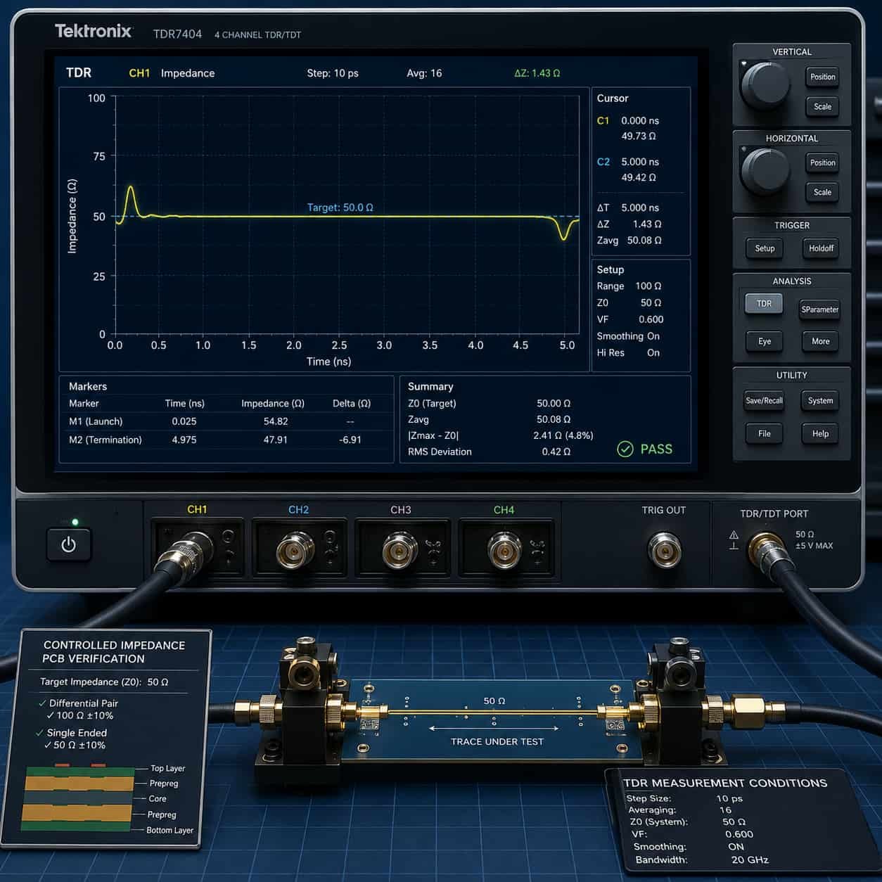
How Factories Verify Controlled Impedance: TDR Testing
Time Domain Reflectometry (TDR) is the industry-standard method for verifying controlled impedance on manufactured PCB. A TDR instrument sends a fast-rise-time pulse down the impedance trace and measures the reflections caused by impedance variations along the trace.
How TDR Works
- A step pulse is launched into the impedance trace
- The TDR instrument measures the reflected signal versus time
- Impedance at each point along the trace is calculated from the reflection coefficient
- The display shows impedance versus distance — a flat line at the target impedance indicates a good trace
- Deviations from flat indicate impedance variations caused by trace width variation, dielectric thickness variation, or material Dk variation
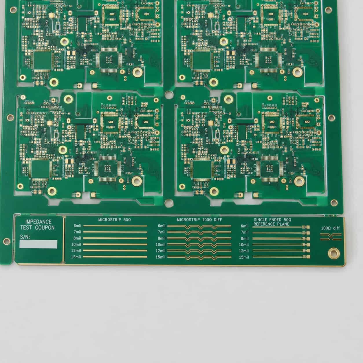
The Impedance Test Coupon
TDR measurement is performed on an impedance test coupon — a dedicated test trace placed on the edge of the production panel that represents the signal layer stackup geometry. The coupon is not a product trace — it is a measurement structure designed for TDR access.
- Coupon design: microstrip or stripline trace of the same width and layer as the product impedance trace
- Length: typically 6–12 inches to provide adequate TDR resolution
- Location: panel edge — outside the product area
- Launch pads: SMA or probe pads at each end for TDR connection
- One coupon per panel: represents the impedance of all boards on that panel
Our TDR Verification Process
- Every production lot: TDR measurement on impedance coupon — no exceptions for Rogers or PTFE boards
- Measurement standard: compared against target impedance ±10% or ±8% as specified
- Records: TDR measurement results kept for every production lot — available on request for aerospace and defense programs
- Out-of-tolerance response: boards are held, root cause identified, and corrective action taken before release
Controlled Impedance Specification: What to Include in Your Order
When submitting a controlled impedance PCB order, the following information must be specified:
- Target impedance value: e.g. 50Ω single-ended or 100Ω differential
- Tolerance: ±10% (standard) or ±8% (advanced) — if not specified, factory assumes ±10%
- Which layer: which copper layer carries the controlled impedance trace
- Transmission line structure: microstrip, stripline, or coplanar waveguide
- Reference trace width: the trace width in the Gerber that should achieve target impedance — factory verifies this in DFM
- Copper weight on the controlled layer: ±1 oz vs 0.5 oz changes the impedance significantly
- Multiple impedance requirements: if different layers have different impedance targets, specify each
Common Controlled Impedance Failures and Root Causes
Impedance Out of Tolerance — Most Common Failure
- Wrong Dk in calculation: factory used nominal Dk instead of confirmed lot Dk — produces systematic offset across all boards on the lot
- Wrong copper weight: trace width calculated for 1 oz but actual copper is 1.2 oz after plating — trace too wide, impedance too low
- Dielectric thickness variation: Rogers laminate thickness varies slightly — confirmed thickness from material certificate should be used, not nominal
- Wrong bonding film in hybrid stackup: standard FR4 prepreg instead of Rogers RO4450F creates Dk discontinuity — impedance shifts at the interface
Impedance Variation Across the Panel
- Etch uniformity: trace width varies across large panels if etch chemistry is not uniform
- Press uniformity: dielectric thickness varies if press temperature or pressure is not uniform across large panels
- Solution: impedance coupon at panel edge identifies lot-level offset but not within-panel variation — for tight tolerance designs, confirm factory panel uniformity capability
Impedance Discontinuities at Via Transitions
- Via stub: unused via barrel extends below the signal layer, creating a capacitive stub that shifts impedance at the via
- Solution: back drill to remove unused via stub for high-frequency designs above 10 GHz
- Anti-pad sizing: ground plane clearance around via affects local impedance — must be sized correctly
For back drill specification, see Back Drill PCB: Via Stub Elimination for High Frequency Designs
Controlled Impedance on Different Materials
Rogers RO4350B (Dk 3.48, FR4-Compatible)
- 50Ω microstrip on 0.508mm, 1 oz: trace width ≈ 1.08mm (43 mil)
- 50Ω microstrip on 0.254mm, 1 oz: trace width ≈ 0.51mm (20 mil)
- Impedance calculation: use confirmed lot Dk from Rogers certificate — nominal 3.48 ±0.05
- Bonding film Dk contribution: Rogers RO4450F Dk ≈ 3.54 — negligible effect on most stackups
Rogers RO3003 (Dk 3.00, PTFE)
- 50Ω microstrip on 0.254mm, 0.5 oz: trace width ≈ 0.30mm (11.8 mil)
- 50Ω microstrip on 0.254mm, 1 oz: trace width ≈ 0.22mm (8.7 mil)
- Impedance calculation: use confirmed lot Dk — nominal 3.00 ±0.04
- PTFE process: plasma activation before plating — affects hole geometry but not trace impedance
Rogers RT5880 (Dk 2.20, PTFE)
- 50Ω microstrip on 0.508mm, 1 oz: trace width ≈ 1.16mm (46 mil)
- 50Ω microstrip on 0.254mm, 1 oz: trace width ≈ 0.55mm (22 mil)
- Impedance calculation: use confirmed lot Dk — nominal 2.20 ±0.02 (tighter tolerance than RO4350B)
- Wide traces at EW frequencies: RT5880’s low Dk produces wider traces with lower conductor loss — EW advantage
For material-specific impedance details, see Rogers RO4350B PCB Guide, Rogers RO3003 PCB Guide, and RF PCB Stackup Design.
Controlled Impedance Capability at Riching PCB
- Standard tolerance: ±10% for traces ≥50Ω; ±5Ω for traces below 50Ω
- Advanced tolerance: ±8%
- Verification: in-house TDR equipment — measured on every production lot
- Calculation: confirmed production Dk from Rogers or Taconic material certificate lot
- Coupon design: factory recommends coupon location and design — included in DFM review
- DFM recalculation: every order recalculated before production — corrections reported before boards are built
- Records: TDR measurement results retained — available for aerospace and defense programs
- Materials: Rogers RO4350B, RO4003C, RO3003, RT5880, Taconic, F4B, ZY — all with confirmed Dk values
- IPC Class 3: impedance verification to IPC-6012 requirements available
For factory capability details, see China High Frequency PCB Manufacturer: Rogers, PTFE, Taconic Direct Factory. For quotation files, see What Files Are Needed for a High Frequency PCB Quotation?.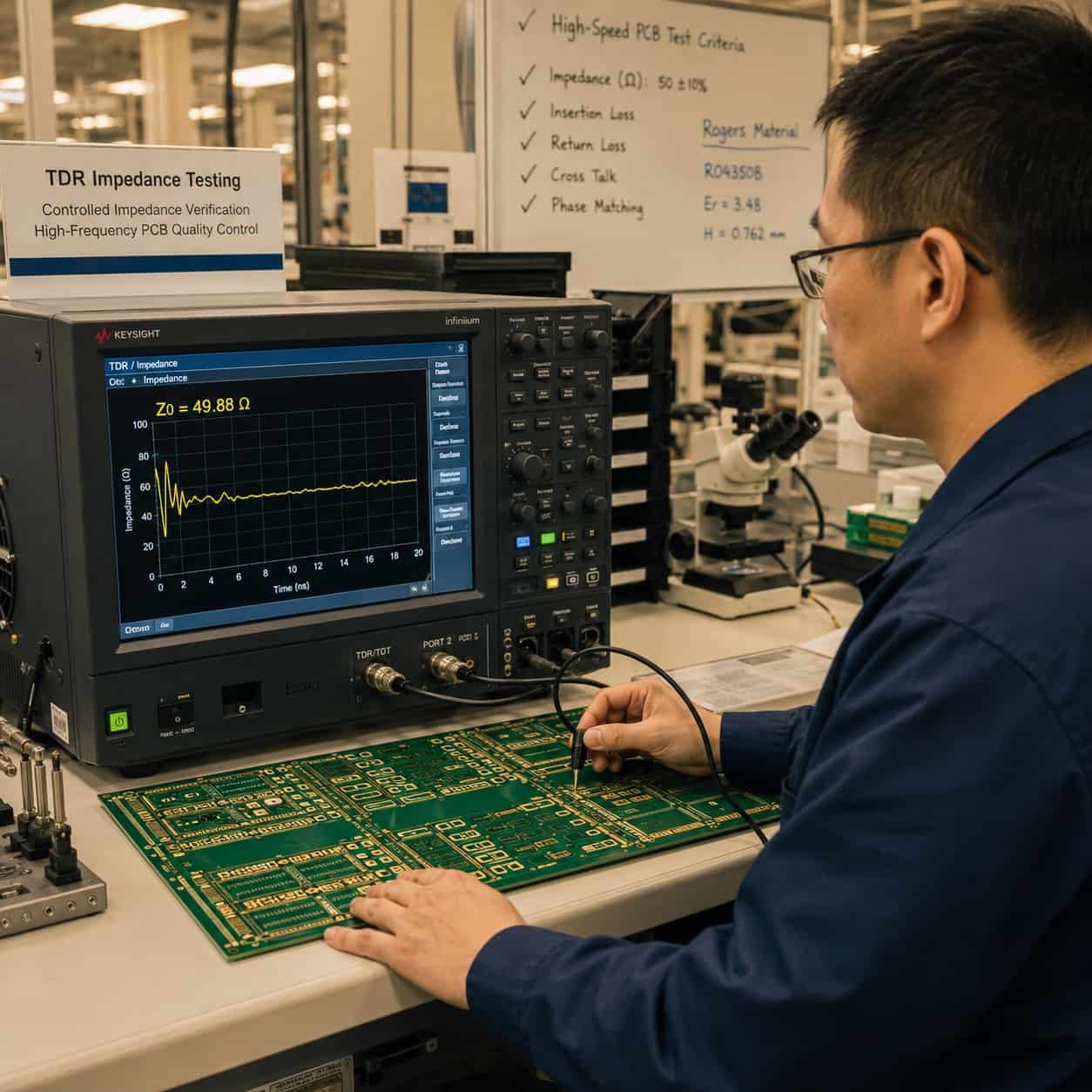
Conclusion
Controlled impedance is a manufacturing process — not just a design calculation. The design calculation determines the target trace width. The factory’s process capability, material Dk verification, and TDR measurement determine whether the manufactured board achieves that target. The most reliable way to get controlled impedance PCB right is to use a factory that recalculates impedance using confirmed production Dk, maintains TDR equipment in-house, and measures every production lot — not as an optional quality step, but as a standard part of the manufacturing process.
As a direct high frequency PCB factory, we do all three for every Rogers, PTFE, and high frequency PCB order. Submit your controlled impedance requirements with your stackup and our engineering team will review the trace width, recalculate using production Dk, and confirm feasibility before production begins.