VSAT PCB and LEO Satellite Terminal PCB: Materials and Manufacturing Guide
PCB substrate selection and manufacturing requirements for GEO VSAT Ku-band terminals and LEO satellite user terminals — Starlink, OneWeb and HTS ground equipment.
Home » Ka-Band PCB » VSAT PCB and LEO Satellite Terminal PCB: Materials and Manufacturing Guide
Table of Contents
Key point: Key point: Most factories quote 3–4 weeks waiting for RO3003 / RT5880 material procurement. Riching PCB maintains these materials in stock — no material wait.
Rogers RO3003 is a PTFE ceramic substrate with Dk 3.0 and Df 0.0010 — standard for Ka-band (26.5–40 GHz), 77 GHz automotive radar and 5G mmWave 28 GHz phased arrays. At 30 GHz, RO3003 insertion loss is ~0.5 dB/cm vs ~1.8 dB/cm for RO4350B. 50Ω microstrip on 0.127 mm RO3003 with 0.5 oz copper: ~0.28 mm trace width. Available thicknesses: 0.127 / 0.254 / 0.508 / 0.762 / 1.524 mm. All RO3003 orders require in-house plasma hole wall activation and maximum 2 lamination press cycles. Riching PCB stocks RO3003 in 0.127 mm and 0.254 mm with in-house plasma activation. No MOQ. Prototype 7–10 working days.GEO VSAT Ku-band PCB (12–18 GHz) uses Rogers RO4350B (Df 0.0037) — FR4-compatible process, no plasma activation required. LEO satellite Ka-band user terminal PCB (17.7–31 GHz) requires PTFE substrate — Rogers RO3003 (Dk 3.0, Df 0.0010) or RT5880 (Dk 2.20, Df 0.0009) — with in-house plasma activation, TDR impedance verification to ±5%, and stable Dk from –40°C to +85°C. Riching PCB stocks RO4350B, RO3003, and RT5880 with in-house plasma activation. No MOQ. Prototype lead time 5–7 days (RO4350B) or 7–10 days (PTFE).
Satellite terminal PCB design has split into two distinct categories driven by the growth of LEO constellations. Traditional GEO VSAT terminals operate at Ku-band (12–18 GHz) with fixed dish antennas — Rogers RO4350B is the standard substrate and the manufacturing process is well established. LEO user terminals for Starlink, OneWeb, and Amazon Kuiper operate at Ka-band (17.7–31 GHz) with electronically steered phased array antennas — PTFE substrate (RO3003 or RT5880), plasma activation, and TDR impedance verification are mandatory.
This guide covers satellite frequency bands, the GEO vs LEO PCB material difference, phased array design requirements for LEO terminals, and manufacturing specifications.
Satellite PCB Frequency Bands
| Satellite Band | Frequency (GHz) | Application | Recommended Material |
|---|---|---|---|
| L-band | 1–2 GHz | Mobile satellite, GPS | RO4350B or FR4 hybrid |
| S-band | 2–4 GHz | Mobile satellite, weather | RO4350B |
| C-band | 4–8 GHz | GEO VSAT, broadcast | RO4350B |
| X-band | 8–12 GHz | Military SATCOM, earth observation | RO4350B or RO3003 |
| Ku-band | 12–18 GHz | GEO VSAT, DTH broadcast | RO4350B or RT5880 |
| Ka-band uplink | 27.5–31 GHz | HTS VSAT, LEO user terminal | RO3003 or RT5880 |
| Ka-band downlink | 17.7–21.2 GHz | HTS VSAT, LEO user terminal | RO3003 or RT5880 |
| V-band | 40–75 GHz | LEO inter-satellite links | RT5880 |
GEO VSAT vs LEO User Terminal PCB
| Parameter | GEO VSAT (Ku-band) | LEO User Terminal (Ka-band) | Notes |
|---|---|---|---|
| Orbit altitude | ~35,786 km | 550–1,200 km | LEO = lower latency |
| Frequency | Ku-band 12–18 GHz | Ka-band 17.7–31 GHz | Ka requires PTFE |
| PCB substrate | RO4350B acceptable | RO3003 or RT5880 required | Ka = PTFE mandatory |
| Antenna type | Fixed dish / flat panel | Phased array / flat panel | LEO = beam steering |
| Temperature range | 0 to +50°C (indoor) | –40 to +85°C (outdoor) | LEO = wider range |
| IPC Class | Class 2 typical | Class 2–3 | Depends on application |
| Plasma activation | Not required (RO4350B) | Required (PTFE) | In-house mandatory |

GEO VSAT PCB (Ku-band, 12–18 GHz)
Traditional GEO VSAT terminals use Ku-band frequencies (12–18 GHz uplink and downlink) with fixed parabolic dish or flat panel antennas. At Ku-band, Rogers RO4350B (Dk 3.48, Df 0.0037) provides acceptable insertion loss for most designs — the relatively short RF trace lengths in a VSAT RF module keep total insertion loss within link budget. RO4350B processes on standard FR4-compatible equipment with no plasma activation required. See RO4350B PCB guide for material properties and stackup design.
LEO Satellite User Terminal PCB (Ka-band, 17.7–31 GHz)
LEO constellation user terminals (Starlink, OneWeb, Amazon Kuiper) operate at Ka-band with electronically steered phased array antennas. Three factors make LEO terminal PCB significantly more demanding than GEO VSAT:
- Ka-band frequency — RO4350B insertion loss is unacceptable at 28 GHz; PTFE substrate (RO3003 or RT5880) is required
- Phased array antenna — hundreds of antenna elements with individual phase shifters, requiring tight impedance uniformity across the entire board
- Outdoor temperature range — LEO terminals operate from –40°C to +85°C, requiring PTFE substrate with stable Dk over temperature
Material Selection for LEO Ka-Band PCB
Rogers RO3003 (Dk 3.0, Df 0.0010) is the standard material for LEO Ka-band user terminal PCB. Its Dk stability over temperature (±0.05 from –40°C to +85°C) is critical for phased array beam steering accuracy — a Dk shift of ±0.05 at 28 GHz moves the antenna element resonance by 300–400 MHz, degrading array gain.
Rogers RT5880 (Dk 2.20, Df 0.0009) offers lower insertion loss and is used for higher-performance terminals or where board area must be minimized. All Ka-band PTFE materials require in-house plasma activation. See Ka-band PCB material guide for detailed comparison.
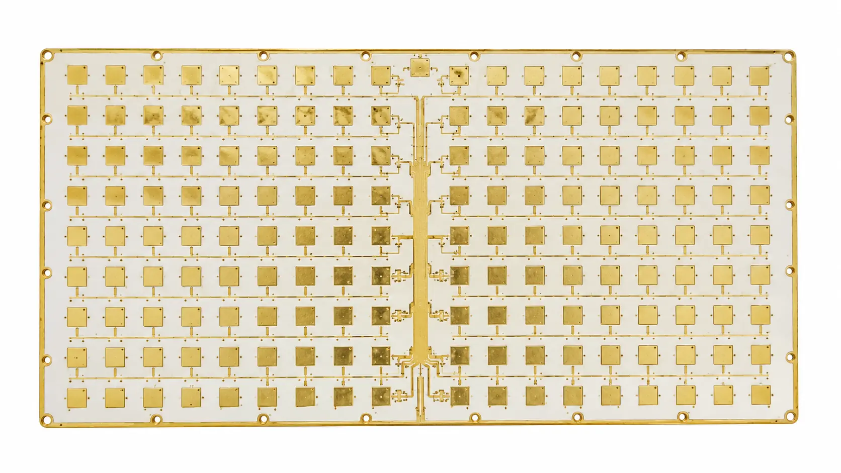
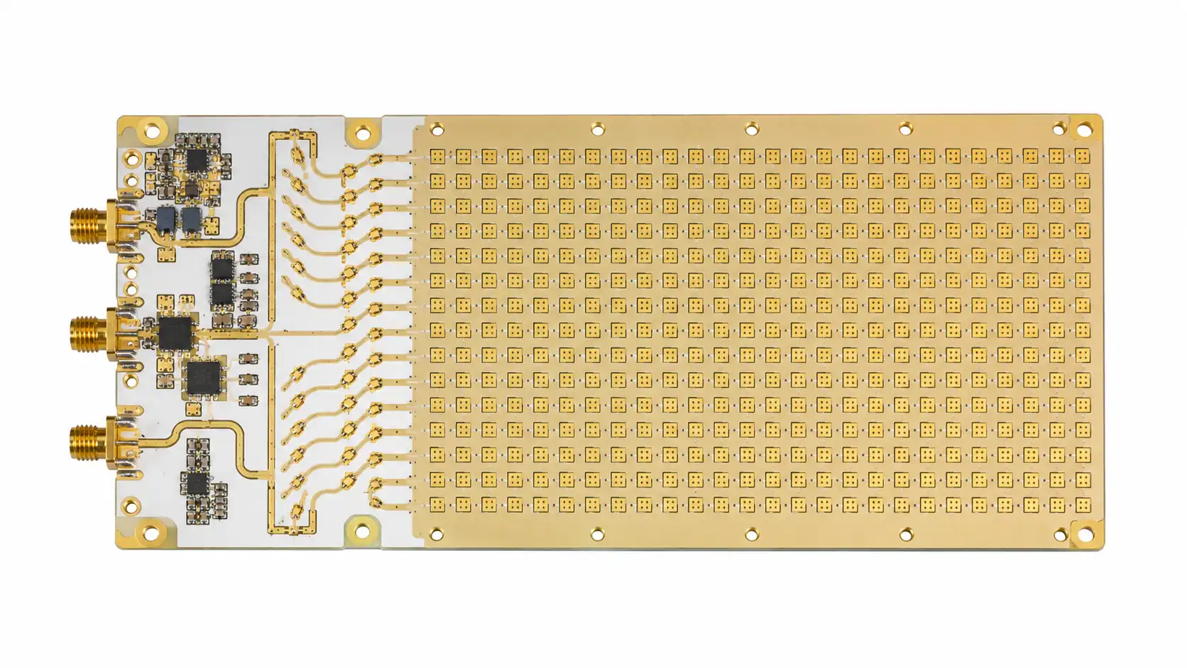
Phased Array PCB Design for LEO Terminals
Antenna Element Design
A typical Ka-band LEO user terminal uses a rectangular patch antenna array with element spacing of approximately λ/2 at the operating frequency — approximately 5 mm at 28 GHz. The feed network distributes RF signal to each element with controlled phase and amplitude. On 0.127 mm RO3003, 50Ω microstrip trace width is approximately 0.28 mm, allowing dense antenna arrays.
Impedance Uniformity
Phased array antenna PCB requires impedance uniformity across the entire board — not just at individual trace level. Dk variation across the panel causes phase errors between antenna elements, degrading beam steering accuracy and array gain. Specify impedance tolerance of ±5% and request TDR verification on multiple points across the panel, not just on edge coupons.
Thermal Management
LEO terminal phased arrays generate significant heat from integrated RF beamforming ICs. The PCB stackup must include thermal vias and copper pours for heat spreading. Rogers RO3003 thermal conductivity (0.50 W/m/K) is higher than RT5880 (0.20 W/m/K) — for high-power phased arrays, RO3003 provides better thermal performance.
Manufacturing Requirements
PTFE Plasma Activation
All Ka-band LEO terminal PCB substrates (RO3003, RT5880) require in-house plasma hole wall activation before copper plating. LEO terminals operate outdoors in temperature cycling from –40°C to +85°C — PTFE PCB without plasma activation fails under thermal cycling. See PTFE PCB manufacturing challenges for full process detail.
Controlled Impedance
±5% impedance tolerance with TDR verification on every production lot. For phased array designs, request TDR verification at multiple locations across the panel to confirm Dk uniformity. Trace width must be calculated from confirmed production Dk certificate.
Surface Finish
ENIG (immersion gold) is standard. For high-volume LEO terminal production, OSP (organic solderability preservative) is used on non-RF pads to reduce cost — specify ENIG on RF signal layers and OSP on digital layers in the surface finish drawing.
Applications

- LEO constellation user terminals — Starlink, OneWeb, Amazon Kuiper CPE
- GEO HTS VSAT terminals — Ka-band high throughput satellite ground equipment
- Maritime VSAT — ship-mounted stabilized antenna systems
- Aero SATCOM — in-flight connectivity antenna PCB
- Military SATCOM — X-band and Ka-band tactical terminal PCB
- Ground station RF equipment — uplink/downlink feed PCB
Conclusion
GEO VSAT Ku-band PCB uses Rogers RO4350B with standard FR4-compatible manufacturing. LEO satellite Ka-band user terminal PCB requires PTFE substrate (RO3003 or RT5880), in-house plasma activation, TDR impedance verification to ±5%, and stable Dk over the –40°C to +85°C outdoor operating range. Riching PCB manufactures both GEO VSAT and LEO terminal PCB — RO4350B, RO3003, and RT5880 in stock, in-house plasma activation, no MOQ. See high frequency PCB capabilities for full factory specifications.
Get a Quote for Your Satellite Terminal PCB
RO4350B, RO3003 and RT5880 in stock. In-house plasma activation. Send the following for DFM review:
- Gerber files + NC drill file
- Application type — GEO VSAT Ku-band or LEO Ka-band terminal
- Material grade and dielectric thickness
- Stackup drawing — copper weight per layer
- Controlled impedance target and tolerance
- IPC Class and quantity
WhatsApp +86 13760473650 — DFM review within 24 hours
Satellite Terminal PCB Q&A
Common questions about VSAT and LEO satellite terminal PCB including GEO vs LEO differences, Ka-band material requirements, phased array impedance and prototype lead times.
What is the difference between GEO VSAT PCB and LEO satellite terminal PCB?
GEO VSAT: Ku-band 12–18 GHz, fixed antenna, RO4350B substrate, FR4-compatible process, no plasma activation. LEO terminal (Starlink, OneWeb, Kuiper): Ka-band 17.7–31 GHz, phased array, PTFE substrate (RO3003 or RT5880) mandatory, in-house plasma activation required, TDR impedance verification to ±5%.
What material is used for LEO satellite user terminal PCB?
Rogers RO3003 (Dk 3.0, Df 0.0010) is standard — Dk stability ±0.05 from –40°C to +85°C is critical for phased array beam steering accuracy. RT5880 (Dk 2.20, Df 0.0009) for lower loss or minimum board area. Both require in-house plasma hole wall activation.
Why does LEO Ka-band PCB require PTFE substrate?
RO4350B (Df 0.0037) produces 3–5 dB/cm insertion loss at 28 GHz — unacceptable for Ka-band feed networks. PTFE (RO3003, RT5880) reduces this to 0.5–1 dB/cm. Dk stability over –40°C to +85°C is also critical — Dk shift moves phased array antenna resonance out of band.
What impedance tolerance is required for phased array satellite PCB?
±5%, verified by TDR at multiple locations across the panel — not just edge coupons. Impedance variation across the panel causes phase errors between antenna elements, degrading beam steering accuracy and array gain. Every production lot must be verified.
What is the prototype lead time for satellite terminal PCB?
RO4350B Ku-band: 5–7 working days. RO3003 / RT5880 Ka-band PTFE: 7–10 working days. No MOQ — from 1 board. DFM review before every order. WhatsApp: +86 13760473650.
Request a PCB Quote
Upload your Gerber ZIP file and project requirements. Our engineering team will review your PCB material, stackup, impedance needs, surface finish, and production quantity before quoting.
Please prepare:
- Gerber files in ZIP format
- PCB material or stackup requirements
- Controlled impedance notes if available
- Prototype or batch production quantity
