
PTFE PCB Field Failures: 5 Manufacturing Mistakes That Pass Testing but Fail in Service
The most dangerous PTFE PCB manufacturing failures are not the ones that get caught at incoming inspection — they are the ones that pass every electrical test, pass TDR, pass cross-section, and then fail after 50–200 thermal cycles in the field. The root cause in almost every case is one of five process errors that are invisible to standard acceptance testing. This article documents each failure mode, how it passes testing, how it eventually fails, and what to verify before placing your next PTFE PCB order.
Home » Controlled Impedance » PTFE PCB Manufacturing Challenges: Plasma Activation, Drilling and Process Solutions
Table of Contents
Key point: Key point: Most factories quote 3–4 weeks waiting for RO3003 / RT5880 material procurement. Riching PCB maintains these materials in stock — no material wait.
Rogers RO3003 is a PTFE ceramic substrate with Dk 3.0 and Df 0.0010 — standard for Ka-band (26.5–40 GHz), 77 GHz automotive radar and 5G mmWave 28 GHz phased arrays. At 30 GHz, RO3003 insertion loss is ~0.5 dB/cm vs ~1.8 dB/cm for RO4350B. 50Ω microstrip on 0.127 mm RO3003 with 0.5 oz copper: ~0.28 mm trace width. Available thicknesses: 0.127 / 0.254 / 0.508 / 0.762 / 1.524 mm. All RO3003 orders require in-house plasma hole wall activation and maximum 2 lamination press cycles. Riching PCB stocks RO3003 in 0.127 mm and 0.254 mm with in-house plasma activation. No MOQ. Prototype 7–10 working days.PTFE PCB manufacturing requires four process steps that standard FR4 equipment cannot perform: plasma or sodium naphthalene hole wall activation before copper plating, PTFE-specific drill parameters at reduced spindle speed, Rogers 2929 bondply for hybrid stackups, and a strict 2-cycle lamination limit. Without plasma activation, copper deposits on the PTFE hole wall with no adhesion — the board passes initial testing and fails under thermal cycling. Riching PCB performs in-house plasma activation on every PTFE order as standard process.
| Failure Mode | Root Cause | How It Passes Testing | How It Fails in Field |
|---|---|---|---|
| Copper delamination | Outsourced plasma or >2hrs before plating | Passes pull test and continuity at room temp | Fails after 50–200 thermal cycles |
| Impedance drift after assembly | SMT reflow above 260°C shifts PTFE Dk | TDR passes before SMT | Impedance shifts 8–15% after first reflow |
| Interlayer delamination | >2 lamination cycles on PTFE stackup | Passes cross-section at delivery | Delamination after field thermal cycling |
| High resistance via | Standard drill speed — PTFE smear | Continuity passes at low current | Via resistance increases under RF power |
| Antenna detuning | PTFE creep under mechanical stress | Antenna resonates correctly on bench | Frequency shifts 2–5% after assembly torque |
Mistake #1 — Outsourced Plasma Activation or Incorrect Timing
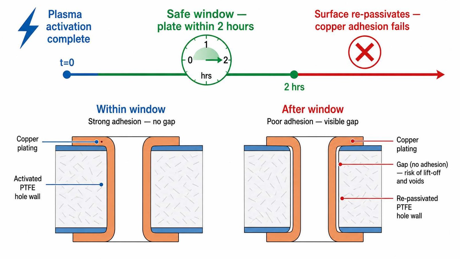
Plasma activation is the process step that makes PTFE bondable to electroless copper. PTFE is chemically inert — without surface treatment, copper deposited on PTFE hole walls has essentially no adhesion and will delaminate under thermal stress. Plasma activation uses an electrical discharge to etch the PTFE surface at the molecular level, creating mechanical interlocking sites for copper nucleation.
▶ Critical: The activated PTFE surface begins to re-passivate (return to its inert state) within 2 hours at room temperature. If more than 2 hours pass between plasma activation and electroless copper plating, adhesion strength drops significantly — but the board will still pass room-temperature pull testing and initial continuity checks.
The failure appears after field thermal cycling. As the board cycles between -40°C and +85°C (or wider), the copper-PTFE interface experiences stress from CTE mismatch. Properly activated PTFE (plated within 2 hours) has sufficient adhesion to survive hundreds of cycles. Late-plated PTFE fails after 50–200 cycles — often in the first 6–12 months of field deployment.
What to verify:
- Ask: ‘Is plasma activation done in-house or outsourced?’ — outsourcing adds transit time that almost certainly violates the 2-hour window
- Ask: ‘What is your documented process time between plasma activation and copper plating?’ — any answer other than ‘≤2 hours, enforced’ is a red flag
- In-house plasma activationwith controlled timing is the correct answer
Mistake #2 — Standard Drill Speed on PTFE
PTFE is mechanically soft — Young’s modulus approximately 0.5 GPa vs 22 GPa for FR4. At standard FR4 drill speeds (typically 80,000–120,000 RPM with standard bit geometry), the drill pushes PTFE material into the hole wall rather than cutting it cleanly. The result is PTFE smear in the hole wall — a thin layer of deformed PTFE covering the hole wall surface.
PTFE drill smear is invisible on standard cross-section inspection unless the lab specifically looks for it. It passes continuity testing at low current. It even passes initial TDR. The failure mode: under RF power, resistive heating at the smeared via increases contact resistance, which increases heating further. The via degrades gradually over months, appearing as increasing insertion loss and eventual thermal failure at higher power levels.
What to verify:
- PTFE-specific drill parameters: 40,000–60,000 RPM spindle speed (lower than FR4, not higher)
- Sharp, new drill bits for PTFE — worn bits produce smear even at correct RPM
- Separate drill programs for PTFE layers in hybrid stackups — not the same program as FR4 layers
Mistake #3 — More Than 2 Lamination Cycles
PTFE materials have a maximum of 2 lamination press cycles. Each lamination cycle subjects the PTFE to elevated temperature and pressure. PTFE begins to flow (creep) above approximately 200°C — during lamination, this causes dimensional changes and stress accumulation in the material. After 2 cycles, the accumulated stress and dimensional change is within acceptable limits. After 3 or more cycles — which is standard for FR4 multilayer designs — PTFE delamination and dimensional instability become significant.
This failure is particularly common in hybrid stackups where a PTFE design is handed to a factory that normally builds FR4 multilayers. The factory applies its standard lamination process (sometimes 3 cycles for complex stackups) to the PTFE layers, producing boards that look perfect at delivery but delaminate in the field.
What to verify:
- Ask: ‘What is the maximum lamination cycles for your PTFE process?’ — correct answer: 2 cycles maximum
- For hybrid PTFE+FR4 stackups: the entire stackup must be designed to be completed within 2 lamination cycles
- Stackup drawing should specify ‘max 2 lamination cycles’ as a manufacturing requirement
Mistake #4 — SMT Reflow Profile Not Modified for PTFE
PTFE begins to soften and exhibit dimensional change above approximately 260°C. Standard SAC305 lead-free reflow profiles peak at 255–260°C — right at the PTFE softening threshold. For PTFE PCB assembly, the reflow profile must be modified: maximum peak temperature 245°C, with reduced time above 230°C.
This failure is subtle: the board passes post-reflow TDR because the Dk shift is small at room temperature. But PTFE that has been heated above its softening point has experienced permanent dimensional change — traces have shifted position by micrometers. At 77GHz, where λ/2 patch spacing is ~1.95mm, a 20μm dimensional shift is a 1% frequency error. Antenna arrays detune. Ka-band filters shift in frequency. The effect is invisible on bench testing but significant in system integration.
What to verify:
- Specify on the assembly drawing: ‘PTFE substrate — modified reflow profile required, max peak 245°C’
- Ask your SMT factory: ‘What reflow profile do you use for RO3003 and RT5880?’ — if they say standard SAC305, correct them before production
- For turnkey PCB+SMT: single factory doing both fab and assembly has the process context to manage this correctly
Mistake #5 — Wrong Bonding Film in Hybrid Stackup
Hybrid PTFE+FR4 stackups require Rogers 2929 bondply at the PTFE-FR4 interface. Standard FR4 prepreg (1080, 2116, 7628 glass styles) does not bond reliably to PTFE surfaces and has different Dk characteristics that create impedance discontinuities at layer transitions. Rogers 2929 is designed specifically for this interface — it bonds to both PTFE and FR4, and its Dk (2.94) is compatible with RO3003 (Dk 3.0) for minimal impedance step at the interface.
Boards built with FR4 prepreg at PTFE interfaces often pass initial electrical testing because the bond is mechanically adequate at room temperature. Field failures occur at the prepreg-PTFE interface after thermal cycling, appearing as delamination at layer transitions in cross-section analysis — but only after the customer has already deployed the product.
What to verify:
- Ask: ‘What bonding film do you use for RO3003 or RT5880 hybrid stackups?’ — correct answer: Rogers 2929 bondply
- Ask: ‘Do you stock Rogers 2929?’ — a factory that regularly builds PTFE hybrid stackups stocks it; one that doesn’t will either order it (adding lead time) or substitute incorrectly
- Rogers 2929 bondply is in stock at Riching PCB for all PTFE hybrid stackup builds
How to Verify Your PTFE PCB Factory Before Ordering
| Question to Ask | ✅ Correct Answer | 🚩 Red Flag |
|---|---|---|
| What hole wall activation method do you use for PTFE? | Plasma activation, in-house | Chemical treatment / outsourced / "standard process" |
| How long between plasma activation and copper plating? | Within 2 hours — enforced | "We do it same day" (vague) |
| What is the maximum lamination cycles for PTFE? | 2 cycles maximum | "Same as FR4" or "3 cycles" |
| What drill RPM do you use for PTFE? | 40,000–60,000 RPM | "Standard parameters" |
| What bonding film for RO3003 hybrid stackup? | Rogers 2929 bondply | FR4 prepreg / "standard prepreg" |
| Do you run TDR on every PTFE lot? | Yes, every panel | "On request only" |
A factory with genuine in-house PTFE capability answers all six questions immediately and specifically. Vague answers, delayed answers, or answers that match FR4 process parameters (3 lamination cycles, standard drill speed, standard prepreg) indicate the factory does not regularly process PTFE materials — regardless of what their website claims.
PTFE PCB Manufacturing Challenges Q&A
Common questions about PTFE PCB field failures, plasma activation timing, lamination cycle limits, bonding film selection and drill parameters.
Why do PTFE PCBs fail in the field after passing testing?
The most common cause is plasma activation timing — if more than 2 hours pass between plasma activation and copper plating, the PTFE surface re-passivates and copper adhesion is weak. The board passes room-temperature testing but fails after 50–200 thermal cycles in the field. Other causes include incorrect drill speed, more than 2 lamination cycles, wrong bonding film in hybrid stackups, and unmodified SMT reflow profile.
How long after plasma activation can PTFE be plated?
Plasma-activated PTFE must be plated with electroless copper within 2 hours. After 2 hours, the activated surface begins to re-passivate and copper adhesion drops significantly. This is why in-house plasma activation — not outsourced — is critical for reliable PTFE PCB manufacturing.
What is the maximum number of lamination cycles for PTFE PCB?
Maximum 2 lamination press cycles for any PTFE material (RO3003, RT5880, Taconic, F4B). Each cycle subjects PTFE to elevated temperature where it begins to flow, causing dimensional change. After 3 or more cycles, delamination and dimensional instability become significant. Hybrid PTFE+FR4 stackups must be designed to complete within 2 cycles.
What bonding film should be used for Rogers RO3003 hybrid stackups?
Rogers 2929 bondply must be used at the RO3003-FR4 interface. Standard FR4 prepreg does not bond reliably to PTFE surfaces and creates Dk discontinuities at layer transitions. Rogers 2929 (Dk 2.94) is compatible with RO3003 (Dk 3.0) and bonds reliably to both materials.
What drill speed should be used for PTFE PCB?
PTFE requires lower spindle speed than FR4 — typically 40,000–60,000 RPM with PTFE-specific bit geometry. At standard FR4 speeds, the drill pushes soft PTFE into the hole wall rather than cutting cleanly, producing drill smear that increases via resistance under RF power.
In-House Plasma Activation — PTFE PCB Without the Field Failure Risk
Riching PCB runs plasma activation in-house with a documented ≤2 hour activation-to-plate window. Max 2 lamination cycles enforced. Rogers 2929 bondply in stock. TDR every lot. RO3003 0.127mm and RT5880 in stock — 7–10 day prototype, no MOQ.
PTFE PCB Manufacturer → WhatsAppRequest a PCB Quote
Upload your Gerber ZIP file and project requirements. Our engineering team will review your PCB material, stackup, impedance needs, surface finish, and production quantity before quoting.
Please prepare:
- Gerber files in ZIP format
- PCB material or stackup requirements
- Controlled impedance notes if available
- Prototype or batch production quantity