
FR4 + Rogers Hybrid PCB: When to Use, Stackup Options and Cost Trade-offs
FR4 + Rogers hybrid PCB: what a hybrid stackup is, when it pays off against a full high-frequency build, the common stackup options, the bonding layer between FR-4 and Rogers material, and the cost trade-offs.
Home » Controlled Impedance » FR4 + Rogers Hybrid PCB: When to Use, Stackup Options and Cost Trade-offs
Table of Contents
An FR4 + Rogers hybrid PCB is a multilayer board that places high-frequency laminate only in the layers that carry RF signals, while FR-4 forms the power, digital and mechanical layers around them. It exists for a practical reason: high-frequency material is specified for its stable dielectric constant and low dissipation factor, and those two properties are only needed in the layers a microwave signal actually travels through.
This guide covers when a hybrid stackup is worth the extra lamination step, the four stackup architectures most RF boards use, how the bonding layer between FR-4 and the RF laminate is chosen, where the cost actually moves, and what to send with a quote request. It is written for RF engineers and buyers specifying boards roughly between 1 GHz and 40 GHz, where a full high-frequency build is not justified.
1. What Is an FR4 + Rogers Hybrid PCB?
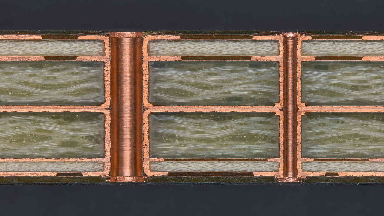
A hybrid PCB stackup combines two or more laminate families in one board. In practice this almost always means high-frequency material in the RF layers and standard FR-4 in the remaining layers, bonded together in a single lamination sequence. The finished board is one mechanical unit — not two boards glued together — with continuous plated through-holes running from the outer layer to the bottom.
The architecture is worth considering because dielectric properties only matter where the electromagnetic field is. A microstrip line on layer 1 couples to its reference plane on layer 2; a stripline on layer 3 couples to the planes on layers 2 and 4. Layers that carry DC power or low-speed digital signals never see the field, so their dielectric constant has no effect on RF loss. The layers that do carry RF, on the other hand, need Dk held to a tight tolerance and a dissipation factor low enough that insertion loss stays inside budget.
Because that difference is what the whole decision rests on, it is worth stating the numbers plainly:
| Laminate family | Dk (with test frequency) | Df (with test frequency) | Thermal | Z-axis CTE | Water absorption |
|---|---|---|---|---|---|
| Standard FR-4 | 4.2–4.6 @ 1 MHz | ≈0.02 @ 1 MHz | Tg 130–180 °C | 50–70 ppm/°C | 0.1–0.3 % |
| RO4350B-class hydrocarbon | 3.48 ±0.05 @ 10 GHz | 0.0037 @ 10 GHz | Tg > 280 °C (TMA) | 32 ppm/°C | 0.06 % |
| RO3003-class PTFE composite | 3.00 ±0.04 @ 10 GHz | 0.0010 @ 10 GHz | PTFE-based, no Tg transition in normal range | 24 ppm/°C | 0.02 % |
Typical datasheet values, listed as facts for stackup planning. Always design against the datasheet of the exact material and lot you specify.
Nothing in that table says one material family is better than another — each is specified for the job it does. What the table shows is why the choice is layer-by-layer and not board-by-board: the RF layers are bought for their electrical tolerance, and the remaining layers are bought for mechanical structure, power distribution and cost.
2. When a Hybrid Stackup Pays Off — and When It Does Not
The decision is not about whether high-frequency laminate is "better". It is about where high-frequency properties are needed and where they are not. Three factors decide it: the number of RF layers relative to total layers, the frequency and loss budget, and the mechanical role of the outer layers.
| Board situation | Stackup that usually fits | Why |
|---|---|---|
| 1–2 RF layers in a 6–10 layer board | Hybrid: high-frequency laminate on the RF layers, FR-4 for the rest | The high-frequency properties are only needed where the field travels; the remaining layers do not benefit from them. |
| RF on both outer layers | Symmetric hybrid: RF outer layers, FR-4 core | A symmetric build balances the two laminate families and limits warp after lamination. |
| More than half the layers carry RF | Single-family high-frequency build | Once most layers need tight Dk and low loss, adding a second laminate family raises process complexity without removing much material cost. |
| All signals below about 500 MHz | Standard FR-4 | FR-4 loss and Dk tolerance are not the limiting factor at these frequencies. |
| RF on one side, heavy connectors, thick board | Hybrid with FR-4 on the mechanical outer layers | FR-4 outer layers give better mechanical robustness for connectors and assembly handling. |
3. Common Hybrid Stackup Options for RF Boards
Most hybrid RF boards fall into one of four architectures. Which one applies is set by where the RF signals enter and leave the board and by how the board is mounted.
| Stackup architecture | Typical layer arrangement | Where it is used |
|---|---|---|
| RF on one surface (most common) | L1 RF signal (RO4350B-class, 10 mil) · L2 RF ground (same family) · L3–L6 FR-4 | RF front ends that share a board with digital control and power. |
| Symmetric RF outer layers | L1–L2 RF (signal + ground) · L3–L4 FR-4 · L5–L6 RF mirrored | Dual-sided feeds, board-to-antenna interfaces, warp-sensitive panels. |
| RF core, FR-4 outer | L1 FR-4 · L2 FR-4 ground · L3–L4 RF stripline core · L5–L6 FR-4 | Stripline RF routing where the outer layers need assembly robustness. |
| Multi-zone RF | Two separate RF layer pairs separated by an FR-4 block | Multi-band boards where two signal groups must stay isolated from each other. |
Two of these deserve a note. The single-surface build is by far the most common because most RF boards carry a front-end section next to digital control logic. The symmetric outer-layer build costs more in RF laminate but is specified when the board is large, thin, or has to stay flat through reflow — the balanced construction is what keeps it from warping.
4. Choosing the Bonding Layer Between FR-4 and Rogers Material
The bonding layer is where hybrid designs most often go wrong. Its dielectric constant and loss factor are part of the RF circuit whenever it sits between an RF trace and that trace's reference plane, and its flow behaviour sets whether the RF laminate and the FR-4 press to the target thickness without resin starvation at the edges.
| Bonding layer | Dk @ 10 GHz | Typical thickness | Where it is used |
|---|---|---|---|
| High-frequency bondply (2929-class) | ≈2.94 | 1.5–4 mil (0.038–0.10 mm) | RF-to-RF and RF-to-FR-4 bonds where the bond line sits inside the RF field and must stay low loss. |
| Low-flow FR-4 prepreg | ≈4.2–4.6 @ 1 MHz | 3–8 mil | Bonds between FR-4 layers, and FR-4 outer layers where the bond line falls outside the RF field. |
The rule of thumb: if the bond line is between the RF trace and its reference plane, it is part of the RF circuit and its Dk and Df matter; if it sits outside the field, a standard low-flow prepreg is the normal choice.
The design-side rules for bonding film selection, lamination cycles and layer placement are covered in more depth in our Rogers FR-4 hybrid PCB design guide, which walks through the specific mistakes that show up at the press.
5. Layer Placement and Reference Plane Rules
Most of the electrical benefit of a hybrid stackup is won or lost in layer assignment, before any manufacturing decision is made. These are the rules that matter most:
| Design rule | Reason |
|---|---|
| Keep the RF layer's reference plane within one dielectric thickness, on the high-frequency side | The field couples across the RF laminate, so the Dk that sets impedance is the high-frequency Dk — not the FR-4 Dk below it. |
| Do not route RF across a plane split | The return current cannot follow the trace, which raises radiation and shifts the effective impedance. |
| Avoid putting the FR-4 / RF interface inside a controlled-impedance field | Dk steps across the interface, so a trace referencing through the boundary behaves as two different electrical thicknesses. |
| Build the stackup symmetrically about the centre line | Balances the CTE mismatch between FR-4 and the RF laminate and reduces warp after lamination. |
| Keep the RF ground plane solid under the RF layer | Segmented grounds change the reference and add inductance in the return path. |
If the goal is to decide whether a hybrid build is right for a new design in the first place, the FR4 + Rogers hybrid stackup guide covers the electrical reasoning behind these rules in detail.
6. Cost Trade-offs: What Hybrid Saves and What It Adds
A hybrid stackup is not simply "the cheaper version" of an all-RF board. It moves cost rather than removing it: the base material bill falls, and the process bill rises. Both sides are real, and both have to be counted:
| Cost item | Direction with a hybrid stackup | What drives it |
|---|---|---|
| Base laminate | Lower | High-frequency laminate is used in one or two layers instead of every layer. |
| Lamination cycles | Higher | A hybrid build usually needs an extra press cycle and a controlled bonding sequence. |
| Bonding film | Higher | High-frequency bondply costs more than standard prepreg. |
| Engineering and stackup review | Higher | Impedance must be verified across the material interface, not on one material alone. |
| Process risk (warp, delamination) | Higher without experience | CTE mismatch between FR-4 and the RF laminate concentrates stress at the interface. |
| Panel scrap on RF material | Lower | Less high-frequency laminate is consumed per board, so less of the expensive material is scrapped. |
The saving shrinks toward zero in three situations: when the RF laminate would have been used in most layers anyway, when the board is small enough that the extra lamination cycle dominates, and when a stackup that is hard to press drives up scrap. For the material side of the comparison, our article on what drives Rogers PCB price compared with FR-4 breaks the cost structure down further.
7. Manufacturing Constraints to Design Around
Four constraints follow from putting two laminate families in one press cycle, and each has a design-side answer.
Coefficient of thermal expansion. The Z-axis CTE of a hydrocarbon laminate is roughly 32 ppm/°C and of an FR-4 in the region of 50–70 ppm/°C. That difference is concentrated at the interface, so an asymmetric stackup stores stress through the whole press cycle. The answer is a balanced construction, not a thicker board.
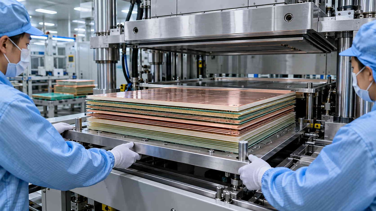
Press temperature and flow. The lamination window has to satisfy both materials at once, which usually means a tighter press recipe than a single-family board needs — and it is the reason a hybrid build will almost always be quoted with an extra press cycle.
Drilling and hole-wall preparation. PTFE-based laminates are softer than FR-4 and smear more readily during drilling, so plasma treatment and a validated desmear sequence are part of the process rather than an option. Hydrocarbon laminates behave closer to FR-4 but still need their own drill parameters.
Watch the asymmetry: an unbalanced hybrid stackup is the most common cause of warp and delamination after lamination. If your stackup drawing carries the RF material on one side only, expect the factory to propose a balancing layer or a thicker prepreg on the opposite side.
The production side of this — lamination sequence, CTE mismatch control and impedance verification across the material boundary — is covered in our guide to how FR-4 and RF laminate are combined in production.
8. What to Send With a Hybrid Stackup Quote Request
A hybrid quote is only as good as the stackup information behind it. Because the quote depends on which layers use which material, the factory needs the layer-by-layer detail rather than a board thickness and a material name. Send these items together:
| Item to include | What the factory needs |
|---|---|
| Stackup drawing | Layer order with the material and finished dielectric thickness for every layer. |
| RF material and Dk tolerance | e.g. RO4350B, 3.48 ±0.05 @ 10 GHz — not just the trade name. |
| Impedance targets | Single-ended and differential values, with the tolerance you will accept. |
| Operating frequency range | The highest frequency the board must carry, so test coverage can be set. |
| Copper weights | Outer and inner layer copper, in oz. |
| Finished thickness and tolerance | Overall board thickness, and thickness on the RF layers specifically. |
| Surface finish | ENIG, hard gold, immersion silver, etc. |
| Build type and quantity | Prototype or production, and the expected repeat volume. |
| Bonding layer preference | If the design already fixes a bondply or prepreg, state it. |
If the stackup is still open on the RF-layer side, say so in the request — it is faster to agree the layer assignment before the quote than to change it afterwards.
FR4 + Rogers Hybrid PCB — Frequently Asked Questions
Short, direct answers to the questions buyers and RF engineers ask before specifying a hybrid stackup.
What is an FR4 + Rogers hybrid PCB?
An FR4 + Rogers hybrid PCB is a multilayer board that uses Rogers high-frequency laminate only in the layers that carry RF signals, while FR-4 forms the remaining power, digital and mechanical layers. The two laminate families are bonded into a single board in one lamination sequence.
Is a hybrid stackup cheaper than an all-RF material board?
The base material cost is lower, because high-frequency laminate is used in one or two layers instead of every layer. That saving is partly offset by an extra lamination cycle, higher-cost bonding film, and tighter process control. Whether the net cost is lower depends mainly on the ratio of RF layers to total layers and on the production quantity.
Can FR-4 and Rogers material be laminated in one board?
Yes. The two materials are bonded with a compatible bonding layer — normally a high-frequency bondply or a low-flow prepreg — in a single lamination sequence. The main process risks are coefficient-of-thermal-expansion mismatch between the materials and thickness control across the interface.
Does the FR-4 portion affect RF performance?
Only if the RF field reaches the FR-4 layers. In a correctly arranged stackup, the RF signal layer references a plane inside the high-frequency material, so the FR-4 layers do not carry the field and their dielectric properties do not enter the loss or impedance calculation.
Need a hybrid stackup reviewed before you release the design?
Send us your stackup drawing and impedance targets. Our engineers check the layer placement, the bonding layer between FR-4 and the RF laminate, and the impedance across the material interface — then quote lamination and lead time on the specific material you specify.
Contact Us → WhatsApp: +86 137 6047 3650Request a PCB Quote
Upload your Gerber ZIP file and project requirements. Our engineering team will review your PCB material, stackup, impedance needs, surface finish, and production quantity before quoting.
Please prepare:
- Gerber files in ZIP format
- PCB material or stackup requirements
- Controlled impedance notes if available
- Prototype or batch production quantity