Most high frequency PCB designs use standard copper weights — half-ounce or one-ounce copper on signal layers. But a significant category of RF and microwave applications requires much thicker copper: high-power RF transmitters, GaN power amplifier modules, radar T/R modules, power distribution networks inside phased array systems, and DC-DC converters that must coexist on the same board as RF circuits.
Heavy copper high frequency PCB — boards with copper weights of 2 oz, 3 oz, 4 oz, or heavier on power-carrying layers — combines the current-handling and heat-spreading capability of thick copper with the controlled impedance and low-loss dielectric performance of Rogers or PTFE materials. The combination requires careful design rule management and manufacturing process control that not all PCB factories can reliably deliver.
As a direct high frequency PCB manufacturer, we produce heavy copper RF boards with copper weights from 0.5 oz up to 6 oz on outer layers and up to 13 oz on inner layers. This guide covers the design rules, manufacturing constraints, and applications for heavy copper high frequency PCB.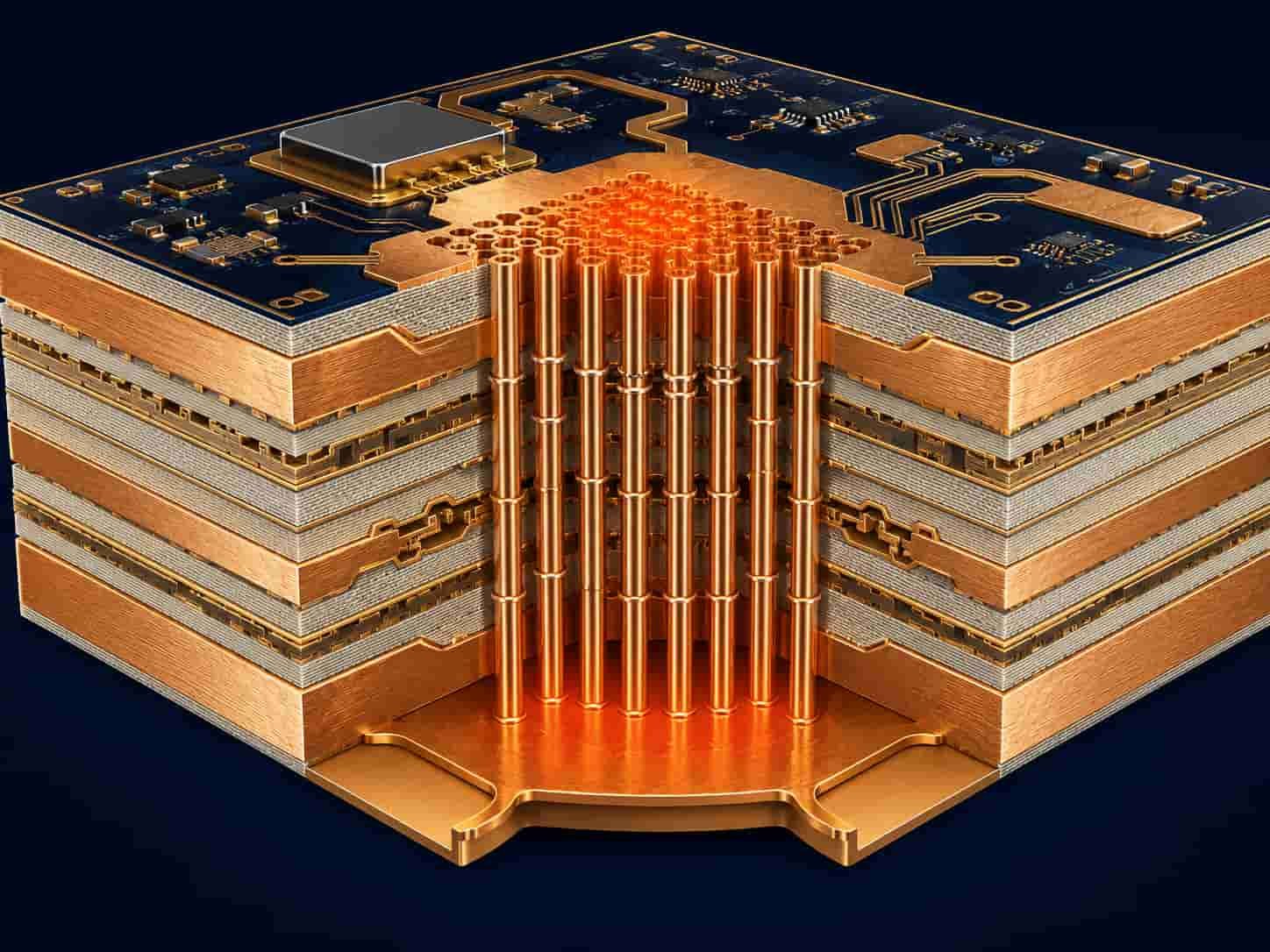
Quick Summary
Key point: Heavy copper high frequency PCB uses 2 oz or heavier copper on power-carrying layers while maintaining 0.5 oz or 1 oz on RF signal layers in the same multilayer stackup. Key manufacturing constraints are minimum line width and spacing by copper weight (wider traces required for heavier copper), etching uniformity across different copper weights on the same layer, and via aspect ratio for thick boards. Our factory capability: outer layer copper 0.5 oz to 5 oz finished, inner layer copper 1 oz to 13 oz, with double-side etch process for 6 oz and above.
The critical design decision for heavy copper high frequency PCB is layer assignment: RF signal layers use standard copper weight for impedance control and line width, while power and ground layers use heavy copper for current capacity and heat spreading. These two requirements are in tension — thick copper on a signal layer widens the minimum trace width and makes fine-pitch impedance control more difficult. Separating these functions across layers resolves the conflict.
Why Heavy Copper Is Used in High Frequency PCB
Heavy copper in high frequency PCB serves distinct functions from the RF signal copper. Understanding these functions helps assign the correct copper weight to each layer in the stackup.
High Current Carrying Capacity
GaN power amplifier chips, radar transmitter modules, and phased array T/R modules all require substantial DC bias current to operate. The PCB power distribution network must carry this current from the power supply to each chip with minimal resistive voltage drop. Thicker copper lowers the resistance of power traces, reducing voltage drop and power dissipation in the distribution network.
- 1 oz copper (35 µm): approximately 3A per mm of trace width for a 10°C temperature rise
- 2 oz copper (70 µm): approximately 4.8A per mm of trace width — 60% more current per mm
- 3 oz copper (105 µm): approximately 6.5A per mm — allows narrower power traces for the same current
- 4 oz copper (140 µm): approximately 8A per mm — used for high current power buses
- GaN T/R module example: a 10W GaN chip at 28V drain voltage draws approximately 0.36A bias per chip — a 100-element array draws 36A total — heavy copper power distribution required
Heat Spreading
In high-power RF PCB, heat generated by active devices must be spread laterally across the copper plane before being conducted through the board to the chassis or heat sink. Thicker copper planes spread heat more effectively than standard 1 oz copper, reducing peak temperatures at the device location.
- Thermal conductivity of copper: 385 W/m·K — much higher than any PCB laminate
- 2 oz copper plane: twice the cross-sectional area of 1 oz — significantly better lateral heat spreading
- Heat spreading reduces peak junction temperature at the chip — extends device lifetime
- Heavy copper inner planes combined with thermal via arrays under chip packages: most effective thermal management approach for high-power RF PCB
Low Inductance Power Distribution
RF power amplifier chips require very low inductance between the DC power supply bypass capacitor and the device power pin. Thicker, wider copper connections have lower inductance than thin traces, reducing high-frequency noise coupling from the switching supply into the RF circuit.
- Power supply noise on the DC rail appears as AM modulation of the RF output — lowers spectral purity
- Heavy copper power planes with close-spaced bypass capacitors minimize power rail impedance at RF frequencies
- Solid copper planes, not routed traces, for power distribution in RF PCB
Applications That Require Heavy Copper in High Frequency PCB
GaN Power Amplifier Modules
GaN (Gallium Nitride) RF power amplifiers are used in radar transmitters, EW jamming systems, satellite uplink terminals, and 5G base station power amplifiers. GaN chips operate at high drain voltages (typically 28V or 48V) and draw significant current. The PCB must support the current path and manage the heat dissipated by the chip.
- Typical GaN chip power dissipation: 5–30W per chip
- Drain current: 0.2–1A per watt of output power
- Heavy copper requirement: 2–4 oz on DC drain supply plane adjacent to chip
- RF signal layers: 0.5–1 oz — standard for impedance control and fine line work
- Thermal via array: 0.2–0.3 mm diameter, 0.5–0.7 mm pitch under chip package
Phased Array Radar T/R Module PCB
AESA phased array radar T/R modules contain multiple GaN or GaAs chips per element. The T/R module PCB must distribute DC power to all chips and manage heat in a compact volume. Large phased arrays with hundreds of T/R elements have very high total power requirements.
- T/R module typical power: 5–50W per element depending on frequency and power level
- 100-element S-band array: 500–5000W total — power distribution PCB must handle substantial current
- Heavy copper on power layers: 2–3 oz standard for T/R module power distribution
- RF layers: 0.5–1 oz on antenna and signal layers
- Rogers RO4350B most common for S-band and X-band T/R module PCB with heavy copper power layers
High-Power Radar Transmitter PCB
Ground-based and airborne radar transmitter PCB must handle the power supply current for the transmitter tube or solid-state power amplifier while also supporting the RF circuit connections. The transmitter PCB may carry kilovolt-level voltages and high currents that require heavy copper with appropriate spacing.
- High-voltage transmitter PCB: heavy copper for high-voltage bus conductors — 4–6 oz common
- High-current bias distribution: 2–4 oz for current paths
- RF circuit layers: standard copper weight — separate from high-power layers
- Creepage and clearance: high-voltage PCB requires minimum spacing between conductors per IPC-2221
Power Electronics + RF Integration
Some RF systems integrate power conversion directly on the RF PCB — DC-DC converters, switching regulators, or power factor correction circuits that supply the RF amplifier chain. These hybrid power + RF boards require heavy copper on the switching power circuit layers and standard copper on the RF signal layers.
- DC-DC converter inductors: often implemented with heavy copper traces or embedded copper bars
- Switching current paths: 2–4 oz copper for low-resistance switching circuit connections
- RF output filter: may share the PCB with the switching circuit — isolation between switching and RF is critical
- EMC challenge: switching transients from the power converter can couple into sensitive RF receive circuits
Copper Weight Options and Minimum Line Width Design Rules
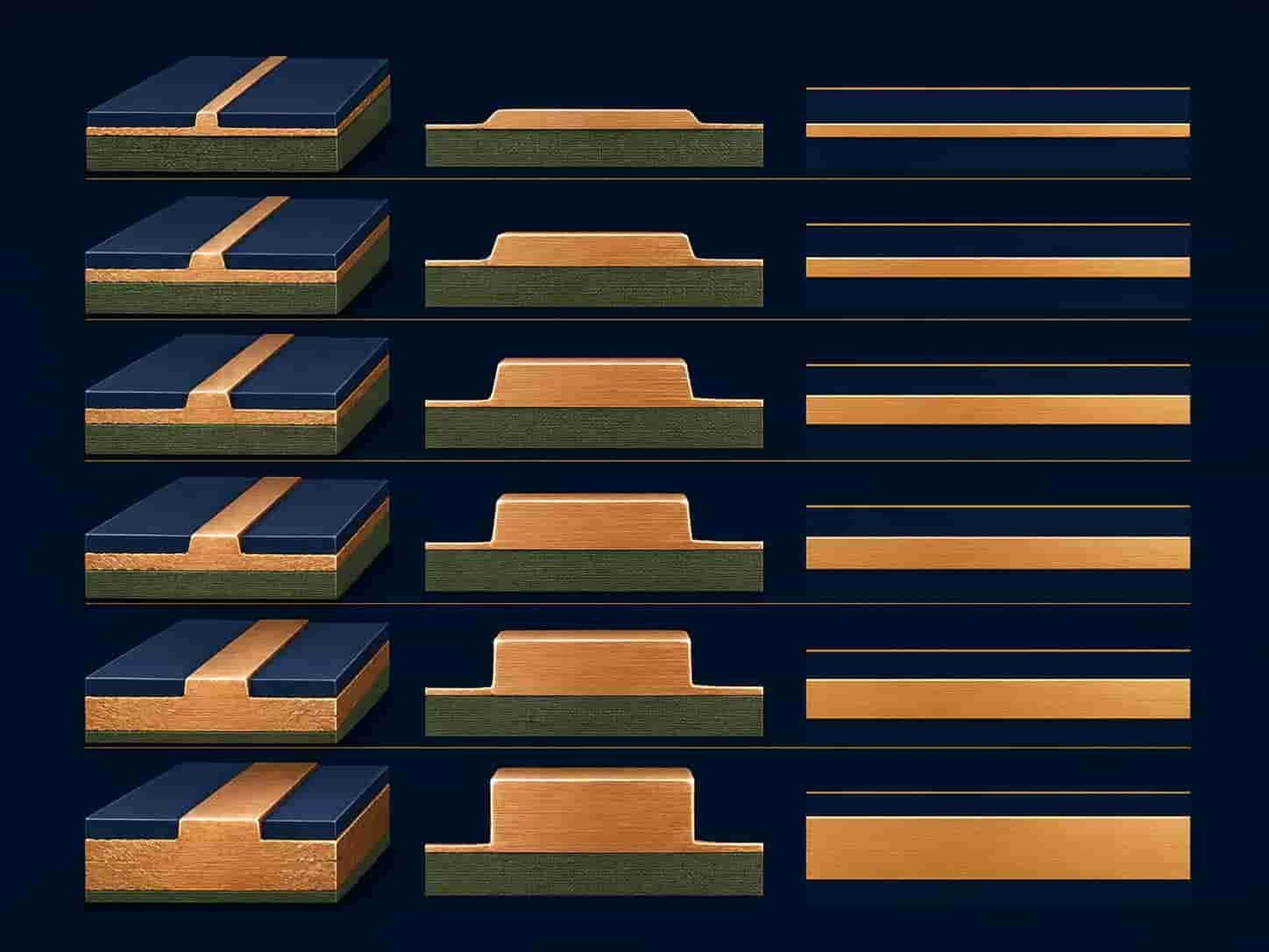
Copper weight directly determines the minimum achievable line width and spacing. Heavier copper requires wider traces because the etching process removes copper from the sides of traces as well as from the surface — the deeper the copper, the more undercut occurs, requiring wider original trace width to achieve the required finished width.
Understanding the Minimum Line Width Requirement
The minimum line width for heavy copper PCB is larger than for standard copper because the etching process creates a trapezoidal trace profile — wider at the bottom, narrower at the top. The etching undercut on each side of the trace is approximately equal to the copper thickness. For 4 oz copper (140 µm thick), the undercut on each side is approximately 140 µm, so the original artwork width must be increased by approximately 280 µm (11 mil) compared to the finished width target.
- 1 oz copper (35 µm): minimum line width 3.5 mil / spacing 3.5 mil standard
- 2 oz copper (70 µm): minimum line width 5 mil / spacing 5 mil
- 3 oz copper (105 µm): minimum line width 6 mil / spacing 7.5 mil
- 4 oz copper (140 µm): minimum line width 9 mil / spacing 11 mil
- 5 oz copper (175 µm): minimum line width 11 mil / spacing 14 mil
- 6 oz copper (210 µm): minimum line width 14 mil / spacing 18 mil — double-side etch process required
Implication for RF Signal Layers with Heavy Copper
The minimum line width constraint of heavy copper directly conflicts with RF impedance control requirements. A 50Ω microstrip on Rogers RO4350B 0.508 mm substrate with 1 oz copper has a trace width of approximately 1.1 mm (43 mil) — well above the heavy copper minimum. However, at Ka-band on thin substrates, the 50Ω trace width may be as narrow as 0.6 mm (24 mil), which approaches or falls below the minimum for 3 oz or 4 oz copper.
- Solution: use standard copper weight (0.5 oz or 1 oz) on RF signal layers, heavy copper only on power and ground layers
- Mixed copper weight stackup: different copper weights on different layers — requires careful lamination process control
- Inner layer copper weight: inner layers can have different copper weight from outer layers — power planes use heavy copper, signal layers use standard
- Verification: confirm that all impedance-controlled traces on RF layers use a copper weight compatible with the trace width requirement
Etching Process Challenges for Heavy Copper High Frequency PCB
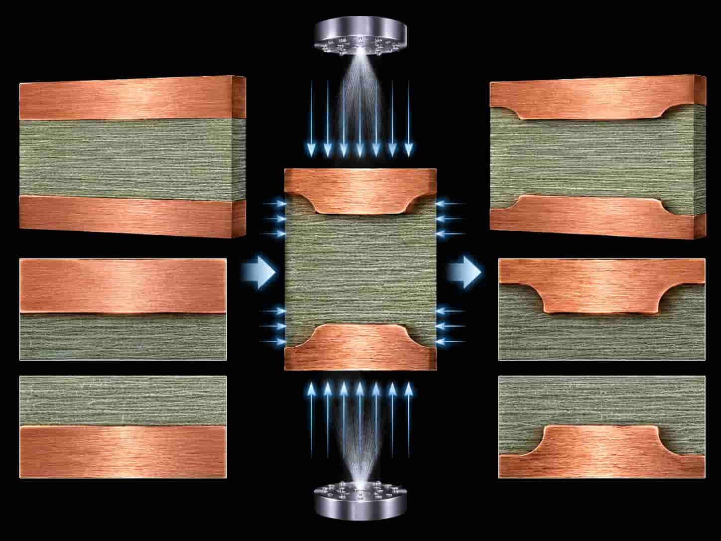
Producing heavy copper PCB requires different etching process parameters than standard copper PCB. The etching challenge increases with copper thickness — heavier copper requires more etch time, which increases lateral undercut and makes line width control more difficult.
Standard Etching vs Double-Side Etch
Standard PCB etching uses a single-sided spray etch where etchant is applied from one side. For copper weights up to 4 oz, single-sided etching with compensated artwork widths produces acceptable results. For 5 oz and 6 oz copper, our factory uses a double-side etch process where etchant is applied simultaneously from both sides of the panel, reducing the required etch time and improving trace profile symmetry.
- Standard single-side etch: suitable for copper weight up to 4 oz (140 µm)
- Double-side etch: required for 5 oz and 6 oz copper — reduces etch time, improves line width control
- Our capability: standard etch up to 4 oz outer layer, double-side etch for 5–6 oz outer layer
- Inner layer heavy copper: up to 13 oz on inner layers — etched before lamination as core copper
Mixed Copper Weight on the Same Layer
Some designs require different copper weights on different areas of the same layer — for example, 4 oz on a power bus conductor and 1 oz on adjacent signal traces. This is achievable but requires a selective plating or etching process and careful DFM review.
- Pattern plating: deposit additional copper selectively in power areas before etching — allows different effective copper weights on the same layer
- Design rule: minimum spacing between heavy copper and standard copper areas must account for the different etch undercut
- Our factory note: mixed copper weight on same layer is possible but requires engineering review and specific process planning — submit design early for DFM
Solder Mask Over Heavy Copper
Standard solder mask is applied as a liquid and cured. Over heavy copper, the solder mask must bridge large step heights between the copper surface and the surrounding laminate. The solder mask bridge width above heavy copper traces is critical for reliability.
- Solder mask bridge: minimum 3 mil for standard copper, wider required for heavy copper
- Step height: 4 oz copper (140 µm) creates a 0.14 mm step — solder mask application requires controlled viscosity
- IPC-6012 requirement: solder mask coverage of trace edges — more difficult to achieve uniformly over heavy copper
- Our factory capability: solder mask over copper up to 6 oz outer layer — confirmed in production
Rogers Material Compatibility with Heavy Copper Layers
Heavy copper PCB using Rogers materials for RF signal layers requires confirming that the Rogers material is compatible with the lamination temperature, pressure, and process required for the heavy copper layers.
Rogers RO4350B with Heavy Copper
Rogers RO4350B is the most compatible Rogers material for heavy copper multilayer PCB. Its Tg of >280°C means it can withstand the lamination cycles required for heavy copper core preparation. Its hydrocarbon ceramic base is compatible with standard FR4 lamination presses.
- Tg >280°C: withstands lamination cycles for heavy copper core preparation
- Compatible with 2–4 oz copper on adjacent layers
- Bonding film: Rogers RO4450F or RO4450T for RO4350B-to-RO4350B and RO4350B-to-FR4 bonding
- Most common configuration: RO4350B on RF signal layers, heavy copper FR4 or copper plane on power layers
Rogers PTFE (RO3003, RT5880) with Heavy Copper
Rogers PTFE materials are compatible with heavy copper layers but require more careful process management. The PTFE lamination process — particularly the press temperature profile — must be compatible with the heavy copper core preparation.
- PTFE lamination: requires specific temperature and pressure profile — heavy copper adjacent layers add thermal mass
- Maximum lamination cycles: 2 cycles for PTFE — heavy copper core must be prepared in cycle 1 before PTFE layers added in cycle 2
- Hole wall activation: PTFE activation process still required regardless of heavy copper on other layers
- Via aspect ratio: thick board due to heavy copper increases via aspect ratio — verify against factory limit
Our Factory Capability: Heavy Copper High Frequency PCB Specifications
As a direct manufacturing factory, we produce heavy copper high frequency PCB with the following confirmed specifications. These are production capability figures — not claimed estimates.
Copper Weight Capability
- Outer layer finished copper: 0.5 oz to 5 oz (standard capability)
- Inner layer copper: 1 oz to 13 oz
- Starting copper + plating method: outer layers start from base copper plus pattern plating to achieve finished weight
- Double-side etch process: available for 6 oz outer layer on special order
Line Width by Copper Weight (Outer Layer)
- 5 oz: minimum 2.5 mil line / 3 mil space (advanced), 3 mil / 4 mil (standard)
- 1 oz: minimum 3.5 mil line / 3.5 mil space (standard)
- 2 oz: minimum 5 mil line / 5 mil space
- 3 oz: minimum 6.5 mil line / 7 mil space
- 4 oz: minimum 9 mil line / 11 mil space
- 5 oz: minimum 11 mil line / 14 mil space
Board Thickness and Aspect Ratio
- Maximum board thickness: 12 mm (advanced), 5.4 mm (standard)
- Maximum aspect ratio: 14:1 (advanced), 10:1 (standard)
- Boards above 9 mm require individual engineering review
- Heavy copper increases board thickness — verify aspect ratio for vias in thick heavy copper boards
Materials Available with Heavy Copper
- Rogers RO4350B + heavy copper FR4 hybrid: most common configuration
- Rogers RO4003C + heavy copper layers: for lower-loss RF with high-power sections
- Rogers RO3003 + heavy copper: for Ka-band with high-power DC distribution
- Full FR4 + heavy copper: for power electronics boards without RF signal layers
For copper thickness effects on RF trace design, see How Copper Thickness Affects RF PCB Line Width and Impedance Control. For multilayer stackup planning, see Multilayer High Frequency PCB: Layer Count, Stackup and Manufacturing Limits.
Key Design Rules for Heavy Copper High Frequency PCB
The following design rules must be followed when designing heavy copper high frequency PCB. Deviating from these rules without factory engineering review typically results in etching defects, impedance failures, or via reliability problems.
Layer Assignment
- RF signal layers: 0.5 oz or 1 oz copper — keeps trace widths compatible with impedance requirements
- Power supply layers: 2–4 oz copper — maximizes current capacity and heat spreading
- Ground reference planes adjacent to RF layers: 1 oz or 2 oz — heavier copper improves heat spreading, slight impedance effect must be calculated
- Outer layer recommendation: RF-facing outer layers use standard copper weight, power-facing layers use heavy copper
Via Design for Heavy Copper Boards
- Board thickness increases with heavy copper layers — verify aspect ratio against factory limit (14:1 advanced, 10:1 standard)
- Thermal vias under GaN chips: 0.2–0.3 mm diameter, connect through heavy copper planes for effective heat extraction
- Via hole sizing: heavy copper layers require larger drilled hole diameter to achieve same finished hole size after plating
- Blind vias: limited to 2 press cycles for PTFE stackups — plan blind via stages before heavy copper core
Spacing Rules for High Voltage Heavy Copper
If the heavy copper carries high voltage (above 100V), IPC-2221 minimum spacing requirements apply based on the voltage level, whether conductors are conformal coated, and the altitude of operation.
- IPC-2221 Table 6-1: minimum spacing from 0.1 mm at 15V uncoated to >12.5 mm above 500V uncoated
- For high-voltage transmitter PCB: confirm creepage and clearance requirements with the PCB manufacturer before layout
- Conformal coating allows reduced spacing at lower voltages — specify coating requirement on fabrication drawing
Information Needed for Heavy Copper High Frequency PCB Quotation
To review feasibility and provide an accurate quotation for heavy copper high frequency PCB, the following information should be prepared:
- Gerber files (all layers) and NC drill files
- Complete PCB stackup with copper weight specified for every layer
- RF material specification — Rogers grade or other high frequency laminate
- Maximum current requirement on power-carrying layers
- Operating voltage on power layers — for creepage and clearance review
- Layer count and total board thickness
- Via structure — through-hole, blind, thermal vias
- Controlled impedance requirements on RF signal layers — target value and tolerance
- GaN chip power dissipation and thermal via density requirement
- Surface finish — ENIG or ENEPIG
- IPC Class requirement — Class 2 or Class 3
- Solder mask over heavy copper confirmation
- Quantity and delivery requirement
For a complete file checklist, see What Files Are Needed for a High Frequency PCB Quotation?. For surface finish selection, see ENIG vs ENEPIG vs Immersion Silver for High Frequency PCB.
Conclusion
Heavy copper high frequency PCB combines thick copper layers for current capacity and heat spreading with Rogers or PTFE dielectric materials for controlled impedance and low RF loss. The key to successful heavy copper RF PCB design is layer assignment — RF signal layers use standard 0.5 oz or 1 oz copper for impedance control, while power distribution and ground planes use 2–4 oz or heavier copper for current handling and thermal management.
Our factory produces heavy copper high frequency PCB with outer layer copper from 0.5 oz to 5 oz and inner layer copper up to 13 oz, combined with Rogers RO4350B, RO4003C, RO3003, and RT5880 RF materials. Line width design rules by copper weight, double-side etch for 6 oz layers, thermal via array design for GaN chips, and controlled impedance on RF signal layers are all standard parts of our heavy copper RF PCB production process. Submit your stackup and Gerber files for engineering review before design finalization to confirm line widths, aspect ratios, and material compatibility.