
LEO Satellite PCB Design Guide — Ka-Band Materials and Thermal Cycling
Low Earth orbit (LEO) satellite terminals and small satellite payloads present a PCB design environment unlike any terrestrial RF application: extreme thermal cycling, vacuum-compatible material requirements, mechanical robustness for launch, and Ka-band RF performance — all in a single board. This guide covers the practical design considerations specific to LEO satellite PCB: material selection for Ka-band feed networks and phased arrays, thermal cycling design rules, outgassing compliance, and hybrid stackup design for mixed RF/digital boards.
Home » LEO Satellite PCB Design Guide — Ka-Band Materials and Thermal Cycling
Table of Contents
Material Selection for LEO Ka-Band Systems
| Material | Dk | Df | LEO Satellite Application |
|---|---|---|---|
| Rogers RO3003 | 3.0 | 0.0010 | Ka-band Tx/Rx feed networks, phased array panels |
| Rogers RT5880 | 2.20 | 0.0009 | Wideband downlink, low-loss antenna feed |
| Rogers RO4350B | 3.48 | 0.0037 | Sub-Ka digital/control layers, hybrid stackup |
| Polyimide (rigid-flex) | 3.4–3.5 | 0.002–0.004 | Deployable panel interconnects, harness flex |
Rogers RO3003 (Dk 3.0, Df 0.0010) is the standard substrate for Ka-band phased array panels — its narrow 50Ω trace width at thin substrate enables λ/2 element spacing for array designs, and its tight Dk tolerance (±0.04) supports element-to-element phase consistency across large panel areas. See Ka-band PCB manufacturer for material stock and stackup options.
Thermal Cycling and Mechanical Design
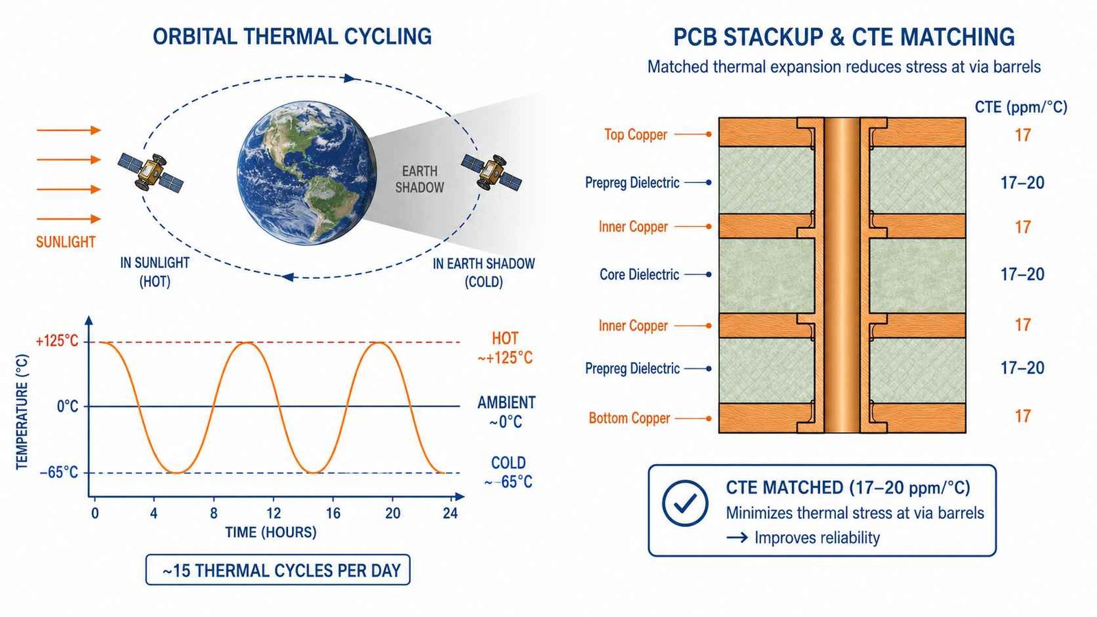
| Design Factor | LEO Environment Driver | Design Response |
|---|---|---|
| Thermal cycling range | Approx. -65°C to +125°C per orbit, ~15 cycles/day | CTE-matched stackup, copper-Dk material pairing, robust via barrel plating |
| Outgassing | Vacuum environment — material outgassing risk | Specify low-outgassing materials, verify TML/CVCM per ASTM E595 |
| Vibration / launch loads | Mechanical stress during launch ascent | Adequate copper anchor, via-in-pad design review, stiffener placement |
| Radiation exposure (TID) | Cumulative ionizing dose over mission life | Substrate is largely radiation-tolerant at LEO TID levels — coordinate with component selection |
| Hybrid stackup transitions | Mixed Rogers + FR4 or polyimide layers | Correct bonding film at each interface — confirm with fabricator before stackup lock |
Why thermal cycling matters more than peak temperature
A LEO satellite passes through Earth’s shadow roughly every 90 minutes, producing a thermal cycle each orbit — approximately 15 cycles per day, or over 5,000 cycles per year. This is fundamentally different from a terrestrial design that might see one or two thermal cycles per day. Fatigue failure mechanisms (via barrel cracking, pad lifting, solder joint fatigue) accumulate with cycle count, not just peak temperature delta. A stackup that survives 100 thermal cycles in qualification testing may not represent the 5,000+ cycles a multi-year LEO mission requires — cycle count in test plans should reflect actual mission duration where possible.
CTE matching across the stackup
In hybrid stackups combining Rogers RF layers with FR4 or polyimide digital/flex layers, CTE mismatch between materials creates stress at via barrels and layer interfaces during thermal cycling. Rogers RO3003 (x-y CTE ~17 ppm/°C) is reasonably well matched to FR4 (~17 ppm/°C) and to copper (~17 ppm/°C) — this matching is one reason RO3003 hybrid stackups are common in satellite payload design rather than introducing additional intermediate materials.
Outgassing Compliance
Materials used in vacuum-exposed assemblies must meet outgassing limits — typically referenced against ASTM E595, with common acceptance criteria of Total Mass Loss (TML) under 1.0% and Collected Volatile Condensable Material (CVCM) under 0.1%. Standard PCB substrate materials (FR4, Rogers laminates) generally meet these criteria, but soldermask formulation, conformal coating, and adhesives used in assembly can be the actual source of outgassing failure. Confirm outgassing data for the complete material stack — substrate, soldermask, coverlay adhesive, and any conformal coating — not just the laminate alone.
Rigid-Flex for Deployable Panel Interconnects
Many small satellite designs use deployable solar panels or antenna elements connected via rigid-flex interconnects rather than discrete cables — reducing connector count and improving reliability under launch vibration. For rigid-flex PCB designs in satellite applications, bend zones experience both the one-time deployment bend and ongoing thermal-cycle-induced flex stress — design bend radius and trace routing accordingly, treating deployment interconnects closer to dynamic-flex design rules than pure static-bend assumptions.
Hybrid Stackup Design Notes
- RO3003 RF layers + FR4 digital layers: bond with Rogers 2929 bondply at the interface, not standard FR4 prepreg
- Maximum lamination cycles for the full stackup is set by the PTFE material — 2 cycles maximum
- Via fence spacing for ground isolation at Ka-band (26.5–40GHz): λ/20 typically requires laser-drilled microvias, not mechanical drilling
- Specify TDR impedance verification (±5% available) for flight or qualification-unit boards — tighter tolerance than typical commercial ±10%
- Document material lot traceability for the full stackup — useful for anomaly investigation if an issue surfaces post-launch
Design Checklist Before Submitting for Fabrication
- Confirm Dk/Df values used in simulation match the actual material certificate, not nominal datasheet values
- Specify bend radius and bend zone clearly on rigid-flex stackup drawings
- Confirm outgassing data availability for substrate, soldermask, and coverlay materials in the stack
- Specify thermal cycling test requirements explicitly if qualification testing will follow — this affects stackup and via design review
- Request a DFM review that addresses both RF performance and thermal/mechanical robustness, not manufacturability alone
LEO Satellite PCB Design — Q&A
Common questions about Ka-band material selection, thermal cycling design rules, outgassing compliance and rigid-flex interconnects for LEO satellite PCB.
What PCB material is used for LEO satellite Ka-band antennas?
Rogers RO3003 (Dk 3.0, Df 0.0010) is the standard substrate for Ka-band phased array panels. Its narrow 50Ω trace width enables λ/2 element spacing, and its tight Dk tolerance supports element-to-element phase consistency across large panel areas.
How many thermal cycles does a LEO satellite PCB experience?
A LEO satellite passes through Earth's shadow approximately every 90 minutes — roughly 15 thermal cycles per day, over 5,000 per year. This requires PCB design to account for cycle-count fatigue (via barrel reliability, CTE-matched materials) rather than just peak temperature.
What outgassing standard applies to satellite PCB materials?
ASTM E595 is the common reference, typically with TML under 1.0% and CVCM under 0.1%. Standard PCB laminates generally meet these criteria, but soldermask, conformal coating and adhesives in the full assembly should also be verified.
Can rigid-flex PCB be used for satellite deployable panel interconnects?
Yes — rigid-flex PCB is commonly used for deployable solar panel and antenna interconnects, reducing connector count and improving reliability under launch vibration. Bend zones should account for both deployment bend and ongoing thermal-cycle flex stress.
Ka-Band PCB for Satellite Terminals — RO3003 In Stock
RO3003 0.127mm and 0.254mm in stock for phased array panels. Rogers 2929 bondply available for hybrid stackups. TDR ±5%, full material traceability. 7–10 day prototype, no MOQ.
Ka-Band PCB Manufacturer → WhatsAppRequest a PCB Quote
Upload your Gerber ZIP file and project requirements. Our engineering team will review your PCB material, stackup, impedance needs, surface finish, and production quantity before quoting.
Please prepare:
- Gerber files in ZIP format
- PCB material or stackup requirements
- Controlled impedance notes if available
- Prototype or batch production quantity