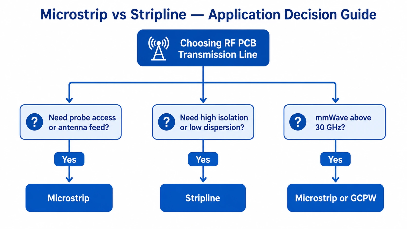
Choosing between microstrip and stripline is one of the first decisions in RF PCB layout. Both structures achieve 50Ω controlled impedance transmission lines, but they have fundamentally different electrical behavior, manufacturing complexity, and application suitability. The wrong choice adds board layers, increases cost, or degrades RF performance.
This guide covers the structural difference between microstrip and stripline, key performance trade-offs, coplanar waveguide (CPW) as a third option, and an application selection guide.
Structure Overview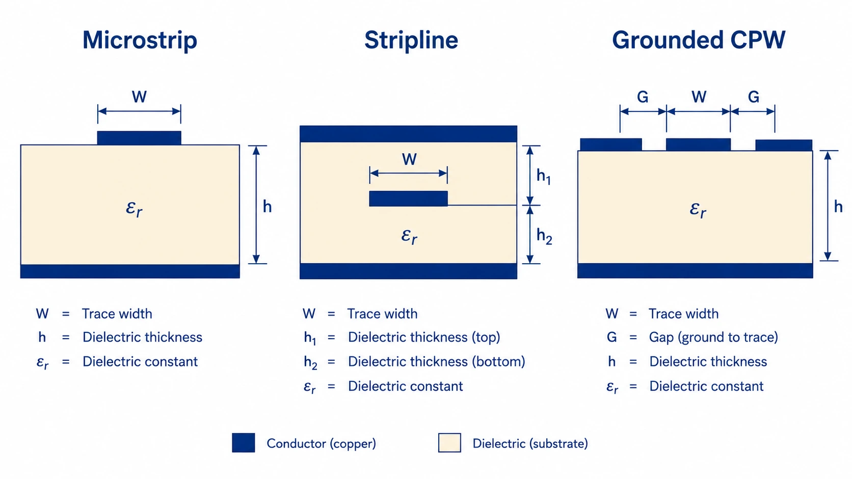
Microstrip
Microstrip is the simplest RF transmission line structure: a signal trace on the outer surface of a PCB above a ground plane reference layer. The electromagnetic field exists partly in the dielectric substrate and partly in the air above the trace. Microstrip requires only 2 PCB layers minimum — signal layer and ground layer. It is the most common structure for single and double-layer RF PCB and for RF circuits on outer layers of multilayer PCB.
Stripline
Stripline buries the signal trace between two ground planes with dielectric above and below. The electromagnetic field is entirely within the dielectric — there is no air interface. Stripline requires a minimum of 4 PCB layers (ground-signal-dielectric-ground). It provides better isolation and lower dispersion than microstrip at the cost of higher layer count, higher manufacturing complexity, and loss of probe access to the buried trace.
Grounded Coplanar Waveguide (GCPW)
GCPW places the signal trace on the outer surface with coplanar ground conductors on the same layer on both sides of the trace, plus a ground plane below. The coplanar grounds provide additional shielding compared to standard microstrip while keeping the trace accessible on the outer surface. GCPW is the standard structure for mmWave PCB above 30 GHz where via transitions in stripline become too lossy.
Microstrip vs Stripline: Detailed Comparison
Insertion Loss
Counterintuitively, microstrip has higher insertion loss than stripline for the same material and frequency. This is because the electromagnetic field in microstrip is split between the dielectric (lossy) and air (lossless). For a given trace length, more field in the dielectric means more dielectric loss. Stripline is fully immersed in dielectric — 100% of the field experiences the substrate Df.
The practical implication: for the same Rogers substrate, a stripline trace has higher insertion loss per unit length than microstrip. Stripline’s isolation advantage comes at an insertion loss penalty. For high-loss materials like FR4, stripline is noticeably worse than microstrip. For low-loss materials like RO3003 (Df 0.0010), the difference is smaller.
Isolation
Stripline provides significantly better isolation between adjacent transmission lines than microstrip. In microstrip, the field extends into the air above the trace and can couple to adjacent structures. In stripline, the ground planes above and below contain the field and prevent radiation coupling. For multi-channel RF modules — receiver front-ends, filter banks, phased array feed networks — stripline reduces cross-coupling between channels by 10–20 dB compared to microstrip.
Dispersion
Microstrip has frequency-dependent phase velocity due to the air/dielectric boundary — the effective Dk changes with frequency. This dispersion causes different frequency components of a wideband signal to travel at different speeds, distorting wideband signals. Stripline, being entirely within a homogeneous dielectric, has much lower dispersion. For wideband EW receivers covering 2–18 GHz, dispersion in microstrip is generally manageable with careful design; for multi-octave signals above 18 GHz, stripline or GCPW is preferred.
Coplanar Waveguide (CPW) and GCPW
CPW places ground conductors on the same layer as the signal trace, with controlled gaps between signal and ground. Grounded CPW (GCPW) adds a ground plane below — combining coplanar isolation with microstrip-like ground reference.
GCPW is the preferred structure for mmWave designs above 30 GHz because:
- Via transitions from the outer layer to inner ground planes introduce inductance that becomes significant above 20 GHz — GCPW reduces via transition requirements
- Coplanar grounds suppress surface wave modes that become significant at Ka-band and above
- Probe pads for on-wafer GSG (Ground-Signal-Ground) probing are naturally compatible with GCPW topology