
Microwave PCB fabrication is not a single process — it is a family of processes that varies significantly depending on the laminate material, layer count, frequency range, and quality standard. A factory that fabricates excellent standard FR4 PCB may not have the process knowledge, equipment calibration, or material handling experience to produce reliable microwave PCB on Rogers or PTFE substrates.
Understanding the microwave PCB fabrication process — what steps are different from FR4, what can go wrong, and what to verify before placing an order — is essential for engineers and buyers who need reliable microwave PCB from prototype through production. As a direct microwave PCB factory producing Rogers, PTFE, Taconic, and F4B boards every week, this guide covers the process from the perspective of the team that runs it.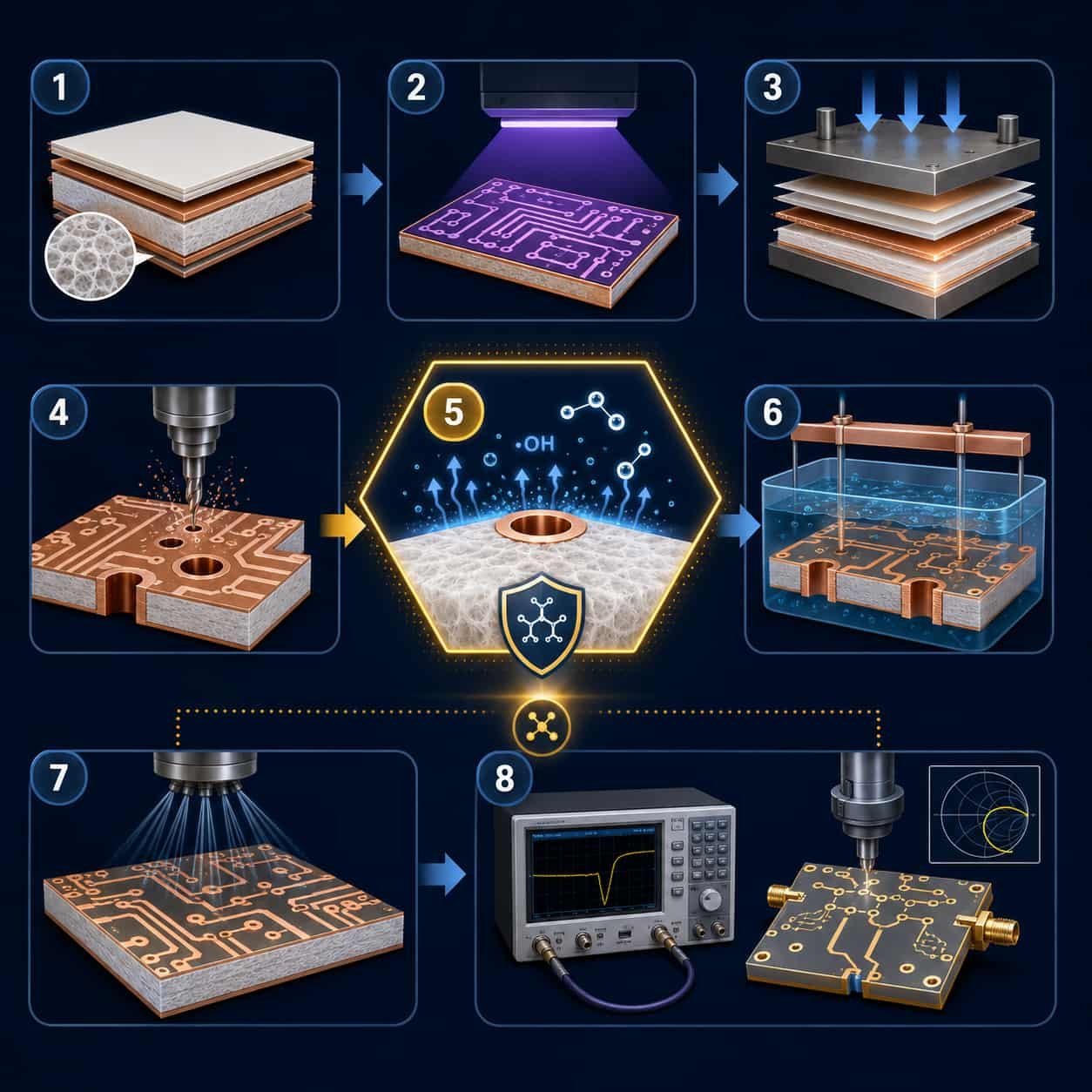
Quick Summary
Key point: Microwave PCB fabrication differs from standard FR4 fabrication in four critical areas: material handling (Rogers laminates are moisture-sensitive and must be stored correctly), lamination (different press profiles and bonding films), drilling (PTFE materials require different parameters than FR4), and hole wall preparation (PTFE requires plasma or sodium activation before copper plating — FR4 and Rogers hydrocarbon do not). A factory that cannot explain exactly how it handles each of these four areas is not reliably fabricating microwave PCB.
What Makes Microwave PCB Fabrication Different from Standard FR4
The fundamental difference between microwave PCB fabrication and standard FR4 fabrication is that every process parameter has tighter tolerances and the consequences of deviation are more severe. An impedance that is 15% off on a digital board causes no visible problem. The same deviation on a microwave filter causes it to pass the wrong frequencies. Copper plating that is 18 µm instead of 25 µm on a digital PCB passes inspection. On a microwave PCB going into an IPC Class 3 aerospace program, it is a reject.
The process differences fall into five categories:
- Material: Rogers and PTFE laminates require different storage, handling, and processing than FR4
- Lamination: different press temperature profiles, bonding films, and cycle limits
- Drilling: PTFE materials require different spindle speed and feed rate — standard FR4 parameters cause hole wall deformation
- Hole wall preparation: PTFE requires plasma or sodium naphthalene activation — FR4 and Rogers hydrocarbon do not
- Impedance control: tighter tolerances, TDR verification on every lot, impedance calculation using confirmed production Dk
Microwave PCB Fabrication: Step-by-Step Process
Step 1: Material Preparation
Microwave PCB fabrication begins with material preparation. Rogers and PTFE laminates require more careful handling than FR4 due to their sensitivity to moisture absorption and dimensional changes.
- Material verification: confirm material grade, lot number, and Dk from the Rogers or Taconic certificate before cutting — production Dk may differ from nominal and affects impedance calculation
- Storage: Rogers hydrocarbon and PTFE laminates should be stored in dry conditions — moisture absorption changes Dk and can cause delamination during lamination
- Cutting: panel cutting to production panel size — Rogers laminates are more brittle than FR4 and require sharper tooling to avoid edge cracking
- Panel size: up to 480×800 mm standard, up to 610×914 mm advanced — large-panel Rogers fabrication for 5G massive MIMO arrays requires confirmed panel handling capability
- Dimensional check: Rogers laminates have lower CTE than FR4 — dimensional changes during processing must be monitored more carefully for fine-pitch designs
Step 2: Inner Layer Imaging
Inner layer imaging transfers the circuit pattern from the artwork to the copper-clad laminate using photolithography.
- Photoresist application: dry film photoresist laminated to inner layer copper surface
- Exposure: UV exposure through phototool transfers circuit pattern
- Development: unexposed photoresist removed, leaving circuit pattern protected
- Etching: exposed copper etched away — for microwave PCB with heavy copper inner layers, etch parameters must account for copper weight
- Strip: photoresist stripped, leaving bare copper circuit
- AOI: automated optical inspection checks for opens, shorts, and dimensional accuracy — critical for fine-pitch microwave circuits
- Minimum inner layer line width: 2.7 mil advanced, 3 mil standard — for fine RF circuit geometry
Step 3: Lamination
Lamination bonds the inner layers and dielectric materials into a multilayer PCB structure using heat and pressure. This is where the most significant process differences between Rogers hydrocarbon and PTFE materials appear.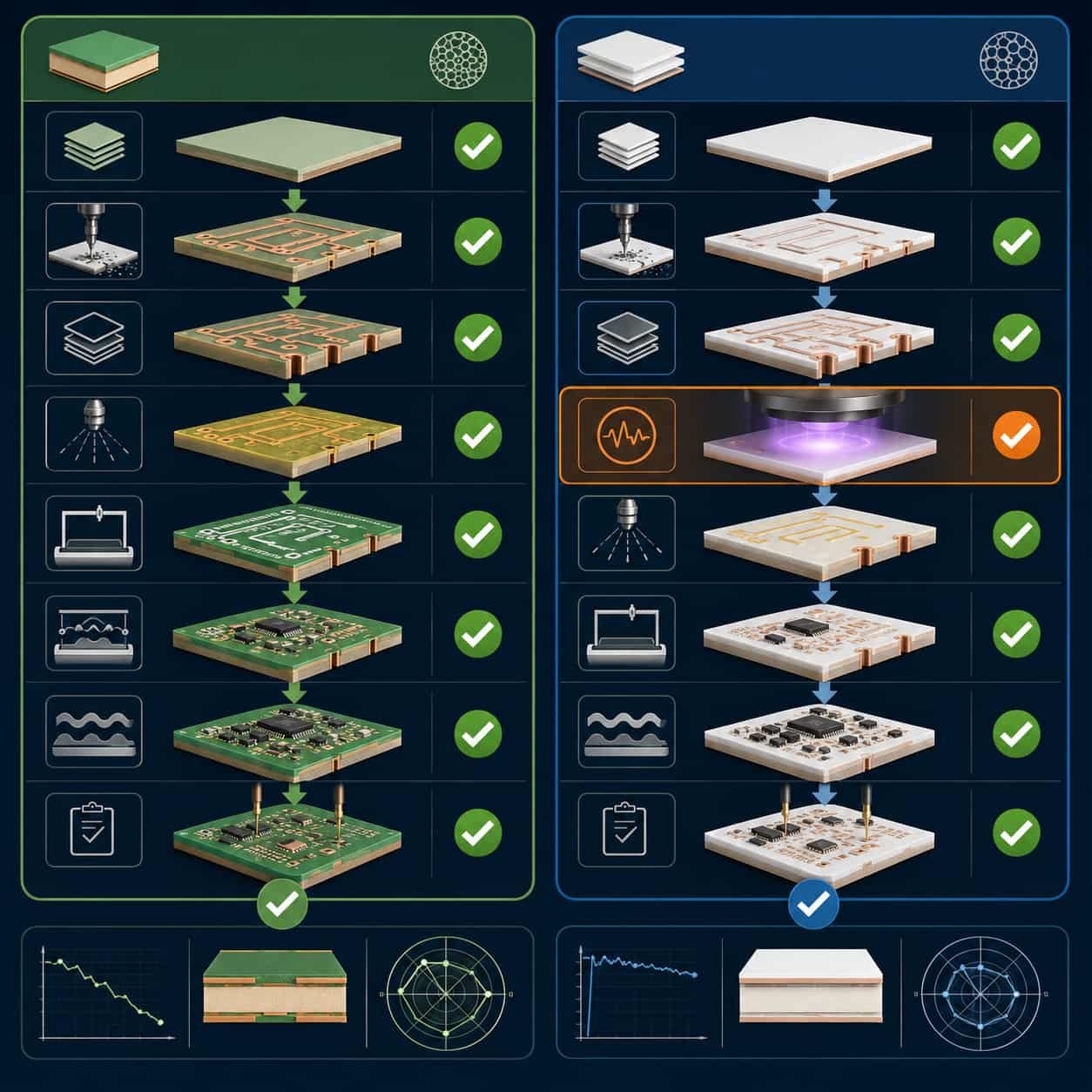
Rogers Hydrocarbon (RO4350B, RO4003C) Lamination
- Press temperature: Rogers-specified temperature profile — different from standard FR4 but uses the same equipment
- Bonding film: Rogers RO4450F or RO4450T bondply between Rogers layers and at Rogers-FR4 interfaces — not standard FR4 prepreg
- Pressure: standard FR4-compatible press pressure
- Maximum cycles: 3 press cycles
- Key check: confirm RO4450F is in factory stock — using standard FR4 prepreg at the Rogers interface is a common error in factories unfamiliar with Rogers fabrication
Rogers PTFE and Taconic PTFE Lamination
- Press temperature profile: PTFE-specific — different from both FR4 and Rogers hydrocarbon
- Press pressure: controlled to prevent PTFE flow — PTFE softens under heat and deforms under excess pressure
- Bonding film: Rogers 2929 bondply for Rogers PTFE, tacBOND for Taconic — not RO4450F, not FR4 prepreg
- Maximum cycles: 2 press cycles only — 3rd cycle degrades PTFE properties
- Dimensional control: PTFE has higher CTE than Rogers hydrocarbon — dimensional verification after lamination
Step 4: Drilling
Drilling creates the via holes and component holes. For microwave PCB, drill accuracy and hole wall quality are critical — especially for PTFE materials.
Rogers Hydrocarbon Drilling
- Parameters: standard FR4-compatible spindle speed and feed rate — no special requirements
- Minimum diameter: 0.2 mm standard, 0.1 mm advanced
- Aspect ratio: 10:1 standard, 14:1 advanced
- Position tolerance: ±0.075 mm standard, ±0.05 mm advanced
PTFE Material Drilling
- Spindle speed: lower than FR4 — PTFE generates heat at the drill tip and smears if RPM is too high
- Feed rate: lower than FR4 — reduces mechanical deformation of the soft PTFE
- Entry and exit materials: PTFE-specific cover and backing boards to prevent burring
- Bit replacement: more frequent than FR4 — PTFE work-hardens drill edges faster
- Hole quality: confirm hole wall smoothness — PTFE drilling defects are more common than FR4 if parameters are not optimized
For drilling capability specifications, see Drilling Capabilities for High Frequency PCB.
Step 5: Hole Wall Preparation — The Critical Difference for PTFE
This is the step that most clearly separates a factory with genuine microwave PCB fabrication capability from one that processes occasional Rogers orders without full PTFE capability.
- FR4 and Rogers hydrocarbon (RO4350B, RO4003C): standard permanganate desmear process — removes resin smear from hole walls, no special activation needed
- PTFE materials (Rogers RO3003, RT5880, Taconic TLY-5, RF-35, F4B): PTFE is chemically inert — copper does not bond to PTFE surfaces without prior activation
- Plasma activation: RF plasma etches the PTFE hole wall surface, creating polar functional groups that accept copper deposition — our factory’s standard method
- Sodium naphthalene: wet chemical alternative — also effective but requires careful chemical handling
- Without activation: electroless copper will not bond reliably to PTFE hole walls — the board passes initial electrical test and fails under thermal cycling when the copper separates from the PTFE
Verification test: Ask any microwave PCB supplier: ‘What hole wall activation method do you use for PTFE materials — plasma or sodium naphthalene?’ A factory that regularly fabricates PTFE PCB will answer immediately and specifically. A factory that doesn’t process PTFE regularly will give a vague answer or ask what you mean.
Step 6: Electroless Copper and Pattern Plating
After hole wall activation (for PTFE) or desmear (for FR4 and Rogers hydrocarbon), a thin layer of electroless copper is deposited to make the hole walls electrically conductive. Pattern plating then builds the copper to the required finished thickness.
- Electroless copper: thin seed layer deposited by chemical reduction — makes PTFE and FR4 hole walls conductive
- Electrolytic copper plating: builds PTH copper to required thickness — 25 µm average for IPC Class 3
- IPC Class 3 requirement: 25 µm average, 20 µm minimum at any point — verified by microsection
- IPC Class 2 requirement: 20 µm average
- Plating distribution: uniform plating thickness from top to bottom of the hole — verified by microsection cross-section
- Void limit: IPC Class 3 allows maximum 5% void per hole, Class 2 allows 10%
Step 7: Outer Layer Imaging and Etching
Outer layer etching defines the final RF circuit geometry — trace widths, impedance-controlled lines, antenna feed structures, and component pads.
- Minimum outer layer line width: 2.5 mil advanced, 3 mil standard — confirmed capability on Rogers and PTFE materials
- Impedance trace compensation: outer layer trace widths are adjusted in the artwork to account for copper weight and etching undercut — the factory must calculate the correct compensation
- Etching tolerance: ±1 mil for traces below 10 mil, ±10% for impedance traces
- Etch uniformity: critical for impedance-controlled traces — non-uniform etching across the panel produces impedance variation between boards
Step 8: Surface Finish
- ENIG: most common for microwave PCB — flat, solderable, corrosion-resistant. Nickel thickness 120–300 µin, gold 1–3 µin.
- ENEPIG: preferred for aerospace and defense IPC Class 3 — eliminates black pad risk
- Immersion Silver: preferred above 10 GHz — no nickel layer, minimum pad resistance
- Immersion Tin: not recommended for microwave PCB — uneven surface affects impedance
- HASL: not recommended for controlled impedance microwave PCB — surface topography variation
Step 9: Solder Mask
- LPI (Liquid Photo-Imageable): standard solder mask for microwave PCB
- Minimum solder mask bridge: 3 mil between pads — 5 mil for non-green colors
- Via tenting: specify whether vias should be tented (covered) or open — for RF PCB, tented vias are common to prevent solder wicking
- Solder mask over RF traces: adds a slight Dk contribution to microstrip impedance — must be accounted for in impedance calculation for designs where this matters
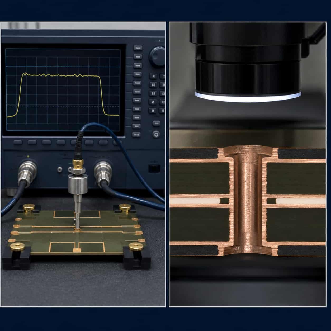
Step 10: Controlled Impedance Testing
Impedance testing is the final verification that the fabricated microwave PCB meets the specified impedance requirements. This is a mandatory step for microwave PCB — not an optional quality check.
- TDR (Time Domain Reflectometry): the standard method — sends a pulse along the impedance coupon and measures the reflection caused by impedance discontinuities
- Coupon design: impedance test coupon placed on the panel edge, representing the actual signal layer stackup geometry
- Measurement frequency: TDR measures at a frequency range that includes the operating frequency of the design
- Tolerance verification: ±10% standard, ±8% advanced — confirmed against the specified target
- Records: TDR measurement records kept for every production lot — available on request for aerospace and defense programs
Quality Standards for Microwave PCB Fabrication
IPC Class 2 vs IPC Class 3
IPC Class 3 is the workmanship standard for aerospace, defense, and high-reliability microwave PCB. The key differences from Class 2 are tighter copper plating requirements, no annular ring breakout, tighter void limits, mandatory 100% electrical test, and required microsection analysis.
First Article Inspection (FAI)
- Microsection analysis: cross-section of representative vias showing copper plating thickness, laminate integrity, and hole wall quality
- Copper plating measurement: average and minimum plating thickness confirmed against IPC Class specification
- Annular ring measurement: internal and external annular rings measured and compared against Class 3 minimum
- Void inspection: voids in PTH copper identified and measured
- Dielectric integrity: no delamination or resin voids in the laminate
- FAI records: retained for program lifetime — 20–30 years for aerospace and defense programs
Electrical Testing
- 100% electrical test: every board tested for continuity and isolation — mandatory for IPC Class 3
- Impedance test: TDR coupon measured on every production panel
- Flying probe or fixture: flying probe for low-volume and prototype, dedicated fixture for production
Common Microwave PCB Fabrication Problems and How to Avoid Them
Impedance Out of Tolerance
The most common microwave PCB fabrication problem. Usually caused by one of:
- Wrong Dk used for impedance calculation: factory used nominal Dk instead of confirmed lot Dk from Rogers certificate
- Bonding film Dk not included: for hybrid stackups, the bonding film Dk contributes to the effective dielectric between layers — factories that use standard FR4 prepreg instead of Rogers RO4450F create an impedance discontinuity
- Copper weight mismatch: impedance calculated for 1 oz copper but actual finished copper is 1.2 oz after plating — trace width needs adjustment
- Etch non-uniformity: traces etched to different widths across the panel — common on large panels with inconsistent etch chemistry
PTH Failure in PTFE PCB
PTH failure in PTFE PCB is almost always caused by skipping or inadequate hole wall activation. The failure mode:
- Board passes initial electrical test — the copper has deposited but has weak adhesion to the PTFE
- Board fails after 50–100 thermal cycles — the weakly bonded copper separates from the PTFE hole wall
- Failure location: at the PTFE-copper interface in the hole barrel
- Prevention: confirm the factory uses plasma or sodium naphthalene activation — ask specifically before ordering
Delamination in Rogers Hybrid Stackups
Delamination between Rogers and FR4 layers in hybrid stackups is caused by using the wrong bonding film.
- Wrong bonding film: standard FR4 prepreg at the Rogers-FR4 interface does not bond reliably to Rogers hydrocarbon surfaces
- Correct bonding film: Rogers RO4450F or RO4450T for RO4350B and RO4003C hybrids
- PTFE hybrid: Rogers 2929 bondply for RO3003 and RT5880 hybrids — different from RO4450F
- Prevention: confirm the factory has RO4450F in inventory and knows which bonding film to use for the specific Rogers material
Microwave PCB Fabrication Capability at Riching PCB
As a direct microwave PCB fabrication factory, we produce Rogers, PTFE, Taconic, F4B, and hybrid microwave PCB in regular production. Our capability covers the full range of microwave PCB fabrication requirements:
Materials
- Rogers hydrocarbon: RO4350B, RO4003C — FR4-compatible process, RO4450F bondply in stock
- Rogers PTFE: RO3003, RO3003G2, RO3006, RO3010, RT5880, RT5870 — plasma activation, 2-cycle limit
- Taconic PTFE: TLY-5A, TLP-5, TLY-5, TLY-3, RF-35, RF-60A, CER-10
- F4B PTFE: F4BM220, F4BM255, F4BM265, F4BM300, F4BTM series
- ZY: ZYF220D, ZYF300CA-P, ZYF350CA and others
- Hybrid: Rogers + FR4, PTFE + FR4, Rogers + Rogers
Process Capability
- Controlled impedance: ±10% standard, ±8% advanced — TDR verified every production lot
- Minimum line width: 2.5 mil outer layer advanced, 3 mil standard
- Minimum drill: 0.1 mm advanced, 0.2 mm standard
- Aspect ratio: 14:1 advanced, 10:1 standard
- Layer count: 2–32 standard, up to 50 advanced
- PTH copper plating: 20–50 µm range, IPC Class 3 25 µm average
- Hole wall activation: plasma — standard for all PTFE materials
- Maximum lamination cycles: 3 for Rogers hydrocarbon, 2 for PTFE
- Panel size: up to 480×800 mm standard, 610×914 mm advanced
- IPC Class: Class 2 standard, Class 3 available
- Surface finish: ENIG, ENEPIG, immersion silver, immersion tin, OSP
- Lead time: 5–7 working days prototype, 10–15 days production
For factory verification guidance, see How to Evaluate a High Frequency PCB Manufacturer. For material selection guidance, see Rogers PCB Material Selection Guide.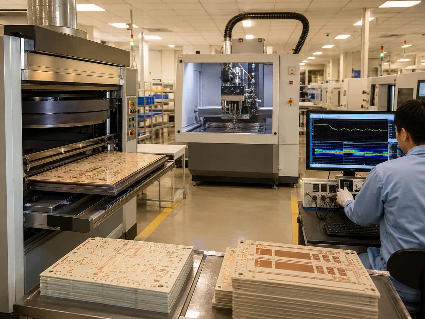
What to Prepare for Microwave PCB Fabrication Quotation
- Gerber files — all copper layers, solder mask, board outline
- NC drill file — all holes, PTH and NPTH separated
- Stackup drawing — material grade, dielectric thickness, copper weight per layer
- Controlled impedance — target value, tolerance, layer, trace structure
- Material specification — Rogers grade or PTFE type
- IPC Class — 2 or 3
- Surface finish
- Layer count and board dimensions
- Application — commercial, aerospace, defense
- Quantity and delivery
For the complete quotation checklist, see What Files Are Needed for a High Frequency PCB Quotation?.
Conclusion
Microwave PCB fabrication requires specific process knowledge and equipment that standard FR4 factories do not have: PTFE hole wall activation for Rogers RO3003 and RT5880, correct bonding film selection for Rogers hybrid stackups, PTFE-specific drill parameters, impedance calculation using confirmed production Dk, and TDR verification on every production lot. These are not incremental improvements to an FR4 process — they are distinct process steps that either exist in a factory or they do not.
As a direct microwave PCB fabrication factory with Rogers, PTFE, Taconic, and F4B production in our own process lines, we produce microwave PCB from 2-layer simple boards through complex multilayer hybrid stackups. Every order goes through engineering DFM review before fabrication begins — confirming material, impedance, and process compatibility before your design is committed to production.