Drilling is one of the most critical process steps in high frequency PCB manufacturing. Every via, plated through-hole, connector hole, and grounding structure starts with a drilled hole. If the drilling process is not controlled correctly, the finished board may have reliability problems, poor RF grounding, connector fit issues, or impedance inconsistency.
For RF PCB, microwave PCB, Rogers PCB, PTFE PCB, and antenna PCB, drilling requirements go beyond standard FR4 PCB production. Material type, board thickness, hole density, via structure, and aspect ratio all affect the drilling process and final board quality.
This guide reviews key drilling parameters, tolerances, aspect ratio limits, PTFE-specific requirements, and what to include in a project review before production.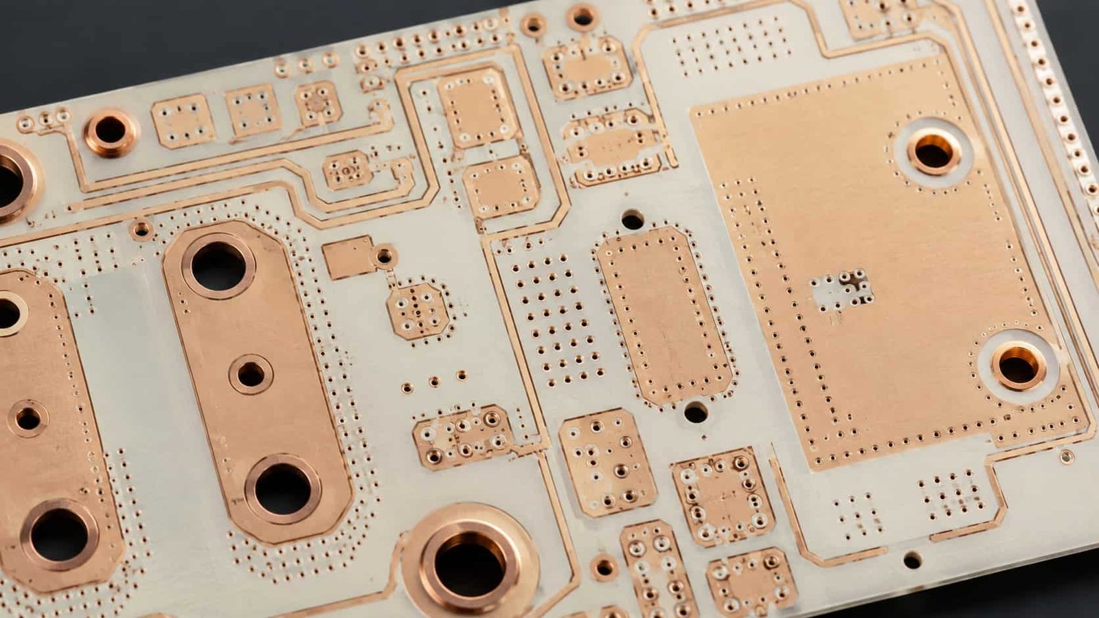
Quick Summary
Key point: Standard mechanical drilling starts at 0.2 mm minimum hole diameter. Advanced capability reaches 0.1 mm. Maximum aspect ratio is 10:1 standard and 14:1 advanced. PTFE materials require a separate process review before drilling.
Drilling requirements for high frequency PCB depend on material type, board thickness, layer count, via structure, and hole density. Projects with fine-pitch vias, high aspect ratio holes, PTFE substrates, or tight positional tolerances should be reviewed by an experienced RF PCB manufacturer before production.
Why Drilling Accuracy Matters for RF and Microwave PCB
In standard FR4 PCB, via holes primarily carry power and digital signals. In RF and microwave PCB, drilled holes also form part of the signal path, ground reference structure, impedance transition, and shielding system.
Drilling errors that might be acceptable in low-frequency digital boards can cause real problems in RF circuits:
- Hole diameter variation changes via pad ring width, which affects RF grounding continuity
- Hole position tolerance affects connector fit and launch geometry, which can shift insertion loss and return loss
- Poor hole wall quality creates unreliable copper plating, which can affect long-term signal integrity
- Incorrect aspect ratio selection increases the risk of plating voids inside deep holes
- Undersized drill selection on thick PTFE boards may cause material deformation or smear
For more background on how via design affects RF performance, see Via Design Considerations for RF PCB Manufacturing.
High Frequency PCB Drilling Specifications
The table below summarizes standard and advanced drilling capabilities for high frequency PCB. PTFE and Rogers PTFE-based materials may require separate review.
Parameter | Standard Capability | Advanced Capability |
Min. drill diameter | 0.2 mm | 0.1 mm |
Hole diameter tolerance | ±0.075–0.08 mm | ±0.05 mm |
Hole position tolerance | ±0.075 mm | ±0.05 mm |
Max. aspect ratio | 10:1 | 14:1 |
PTFE board max. aspect ratio | 8:1 | 10:1 |
Min. hole-to-hole distance (same net) | ≥6 mil | ≥6 mil |
Min. hole-to-hole distance (diff. net) | ≥10 mil | ≥10 mil |
Copper plating in hole (PTH) | ≥20 µm | 20–50 µm |
Note: Advanced capability specifications require engineering review before order confirmation. Not all designs automatically qualify for minimum hole sizes or maximum aspect ratios. Board thickness, material, and panel density all affect feasibility.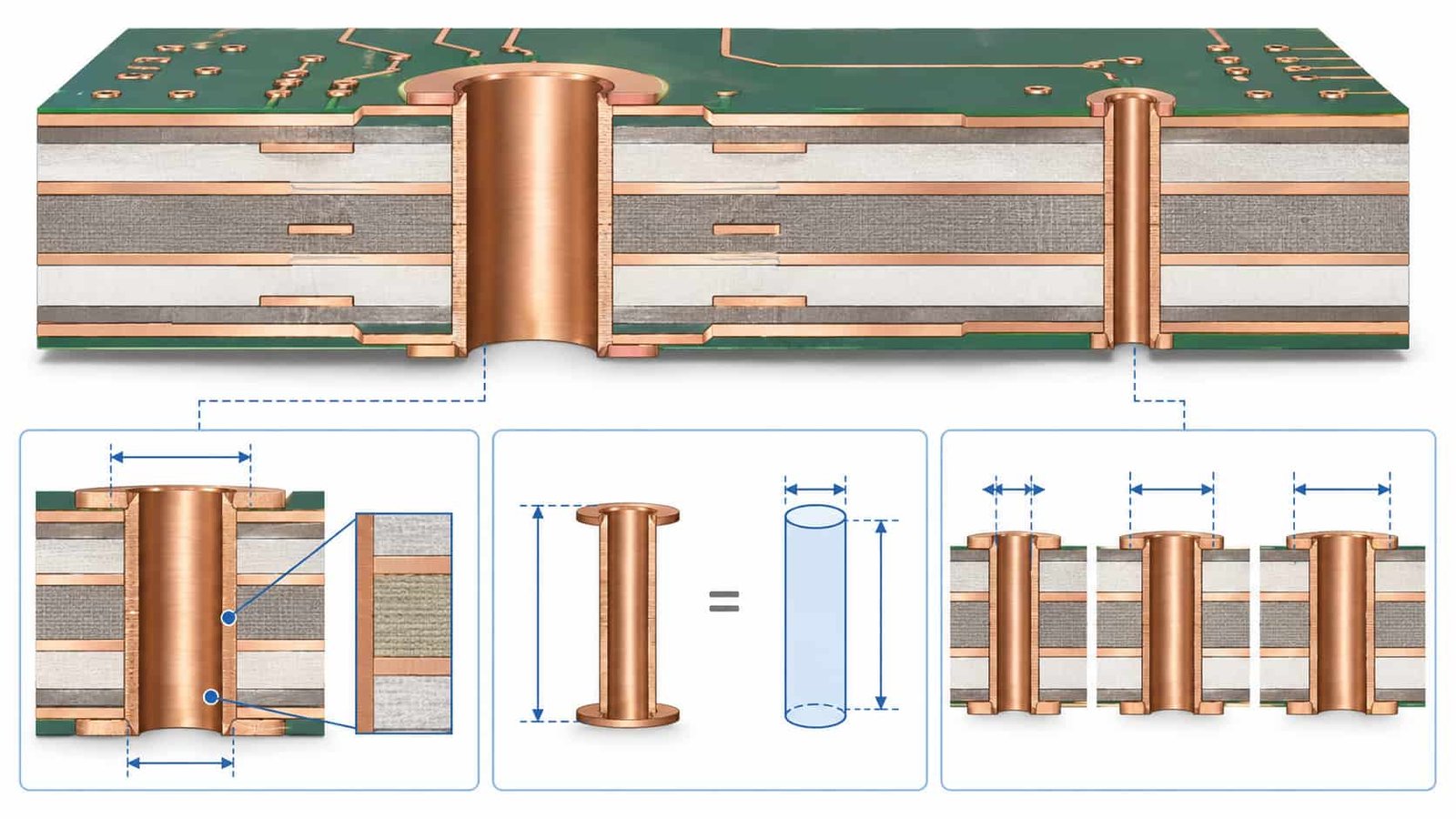
Minimum Drill Size for High Frequency PCB
The minimum mechanical drill diameter for standard high frequency PCB production is 0.2 mm. Advanced manufacturing capability can reach 0.1 mm, but this requires engineering review depending on board thickness, layer count, and material.
For RF and microwave PCB, common reasons for small drill sizes include:
- Via fences for signal isolation between RF traces
- Shielding via arrays around sensitive RF structures
- Fine-pitch component holes in compact RF modules
- Blind via connections in HDI high frequency PCB
- Ground via arrays under RF components and under connector pads
When hole diameter is reduced, the aspect ratio (board thickness divided by hole diameter) increases. High aspect ratios make copper plating inside the hole more difficult and increase the risk of plating voids. This is why minimum drill size and board thickness must always be reviewed together.
For projects with blind via requirements, see also Blind and Buried Via Capabilities in High Frequency PCB Manufacturing.
Aspect Ratio in High Frequency PCB Drilling
Aspect ratio is the ratio of board thickness to drilled hole diameter. It is one of the most important drilling parameters to verify before production.
A high aspect ratio means a narrow hole relative to board thickness. Copper plating must reach deep inside the hole wall from both ends. If the aspect ratio is too high, plating distribution may be uneven, which increases the risk of voids, weak spots, or open connections inside the via.
Aspect Ratio Limits by Material
- Standard FR4-based high frequency PCB: up to 10:1 standard, 14:1 advanced capability
- Rogers PTFE-based materials: lower aspect ratio recommended, typically reviewed case by case
- PTFE composite materials (e.g. RT5880, RO3003): requires separate process review
- F4B and Taconic PTFE materials: follow PTFE-specific guidelines
- Hybrid FR4 + Rogers stackups: governed by thickest dielectric section
Design tip: If your board is 3.2 mm thick and your via hole is 0.3 mm in diameter, the aspect ratio is approximately 10.7:1. This is at the boundary of standard capability and should be reviewed with the manufacturer before finalizing the stackup.
Hole Diameter and Position Tolerances
Hole Diameter Tolerance
Hole diameter tolerance affects via pad ring width, connector fit, press-fit component installation, and final annular ring dimensions after plating.
- Standard capability: ±0.075 mm to ±0.08 mm
- Advanced capability: ±0.05 mm
Tight diameter tolerance is important for RF connector holes, press-fit connector areas, and fine-pitch via arrays where pad ring width is critical for reliable copper plating.
Hole Position Tolerance
Hole position tolerance controls how accurately the drilled hole lands on the design target location. It affects layer registration, via pad coverage, and connector alignment.
- Standard capability: ±0.075 mm
- Advanced capability: ±0.05 mm
For RF connector areas and antenna feed structures, tight position tolerance is recommended to ensure connector launch geometry and controlled impedance consistency.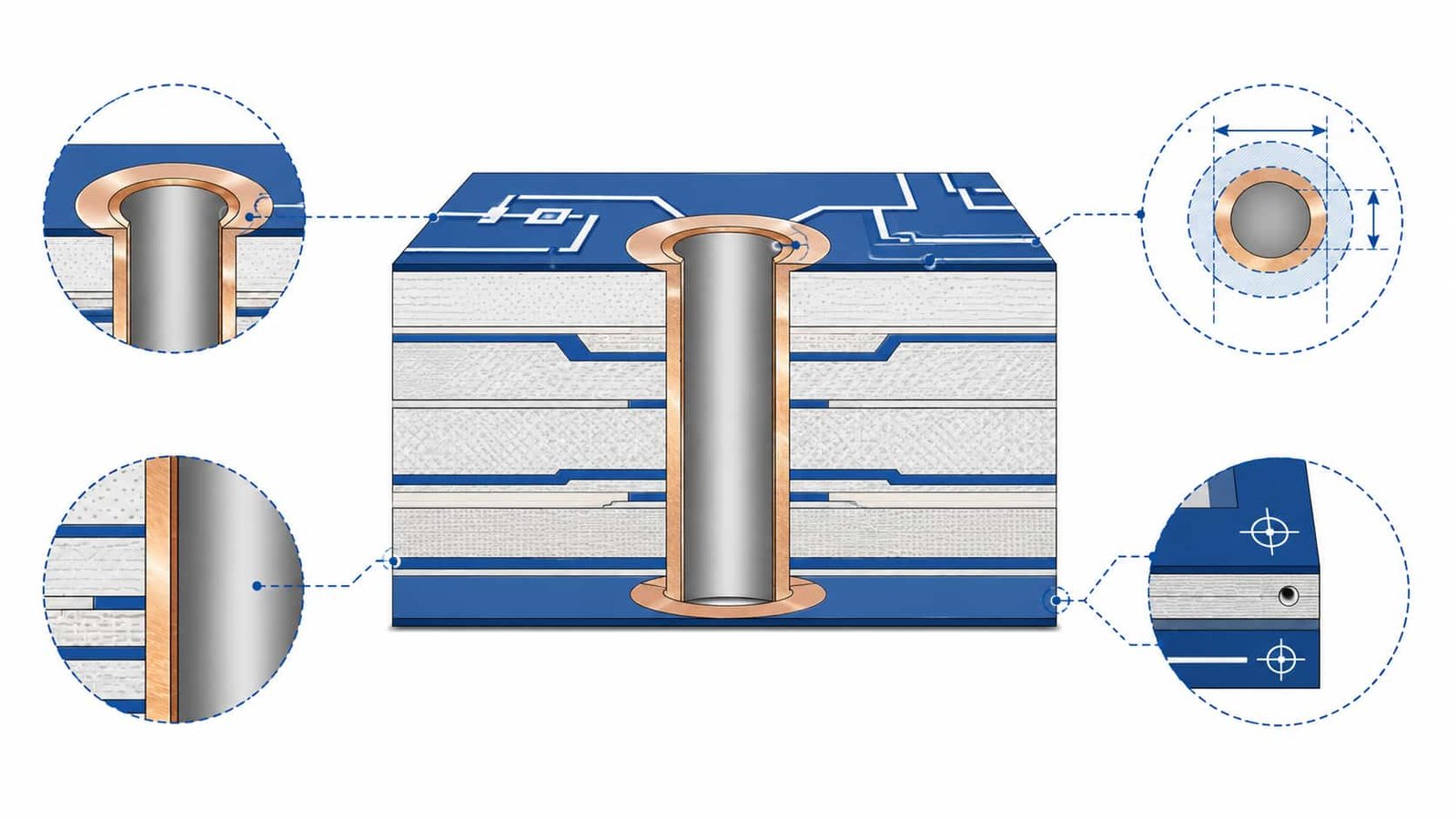
PTFE PCB Drilling: Special Requirements
PTFE-based high frequency materials require different drilling parameters compared to standard FR4 or even Rogers hydrocarbon ceramic materials like RO4350B.
PTFE materials are softer and more elastic than FR4. If standard drill parameters are applied, the material may deform during drilling, creating rough hole walls, smear, or inconsistent hole geometry. This affects plated through-hole reliability and RF via performance.
Key PTFE Drilling Considerations
- Lower spindle speed and feed rate compared to FR4 drilling
- Use of sharp, new drill bits to minimize heat and deformation
- Entry and exit material (cover sheets and backer boards) must be selected for PTFE
- Hole wall must be activated before copper plating — standard FR4 desmear process is not sufficient
- Sodium naphthalene or plasma etching is typically used for PTFE hole wall preparation before seed layer deposition
- Aspect ratio limits are lower than FR4 — standard PTFE capability typically reviewed at 8:1 or lower depending on material
For more detail on PTFE manufacturing requirements, see PTFE PCB Manufacturing Challenges and Process Considerations.
Via Fences, Grounding Vias and RF Via Arrays
In high frequency PCB, drilling is not only about signal connections. Many drilled holes serve as RF shielding, ground references, and signal isolation structures.
Common RF Via Structures
- Via fences along RF traces to suppress signal coupling and crosstalk
- Ground via arrays under RF pads and component footprints
- Connector grounding vias around SMA and MMCX launch areas
- Shielding via walls between RF channels in multichannel designs
- Thermal relief vias under power components in RF amplifier circuits
For via fence design, the spacing between vias is typically kept below λ/20 at the working frequency to maintain shielding effectiveness. This often means small via diameter, tight via pitch, and high via density — all of which depend on drilling capability.
For antenna PCB via grounding design, see Antenna PCB for Wireless Devices and RF Front-End Modules.
Connector and Press-Fit Hole Requirements
RF connector holes are among the most tolerance-critical drilled features in high frequency PCB. SMA, MMCX, SMP, and other RF connectors require accurate hole diameter and position to ensure proper mechanical fit, electrical grounding, and signal launch geometry.
- Standard press-fit connector holes: tolerance ±0.05 mm for reliable mechanical retention
- SMA through-hole connector flange grounding: position tolerance ±0.05 mm recommended
- Connector center pin hole: diameter and position must match connector datasheet
- Solder-through RF connector holes: inner diameter and pad ring must be confirmed in stackup review
For full connector launch and RF layout review requirements, see RF PCB Stackup Design: Key Factors Before Manufacturing.
Drilling Information Needed for High Frequency PCB Quotation
To review drilling feasibility and quote accurately, the following information should be provided:
- Gerber files (all layers)
- NC drill files in Excellon format
- PCB stackup with total board thickness
- Layer count and via structure (through-hole only, blind, buried, or combination)
- Material type — FR4, Rogers, PTFE, Taconic, F4B, or hybrid
- Smallest hole diameter and highest aspect ratio via
- Controlled impedance requirements
- Surface finish requirement
- Quantity — prototype or batch
- Working frequency or application background
For a full quotation checklist, see What Files Are Needed for a High Frequency PCB Quotation?.
Conclusion
Drilling capability is a fundamental part of high frequency PCB manufacturing quality. Minimum hole size, aspect ratio, diameter tolerance, position tolerance, and PTFE-specific process requirements all need to be verified before production.
Projects using Rogers PCB, PTFE PCB, or hybrid stackups should include drilling review as part of the standard pre-production engineering check. Early review reduces rework risk, improves prototype success rate, and supports consistent batch production.
─────────────────────────────────────────────────────────