Missile guidance and seeker systems represent the most demanding combination of high frequency PCB requirements in defense electronics. The PCB inside a missile seeker must operate at Ka-band or W-band frequencies, fit within a highly constrained cylindrical volume, survive launch acceleration forces measured in hundreds or thousands of g, function across extreme temperature ranges from cold storage to aerodynamic heating, and operate reliably for the duration of the mission with zero possibility of repair after launch.
These requirements drive material selection, stackup design, manufacturing quality, and environmental qualification to the highest levels in the high frequency PCB industry. Rogers RO3003 and RT5880 are the standard materials for most missile seeker PCB applications. IPC Class 3 workmanship is the baseline, and many programs impose additional requirements above Class 3 for the most critical guidance electronics. Understanding these requirements is essential for anyone involved in specifying or procuring high frequency PCB for missile guidance and seeker applications.
This guide covers seeker system types and frequency requirements, Rogers material selection for missile PCB, miniaturization and compact design constraints, environmental qualification including high-g shock and vibration, thermal management, IPC Class 3 requirements, and what to confirm before production.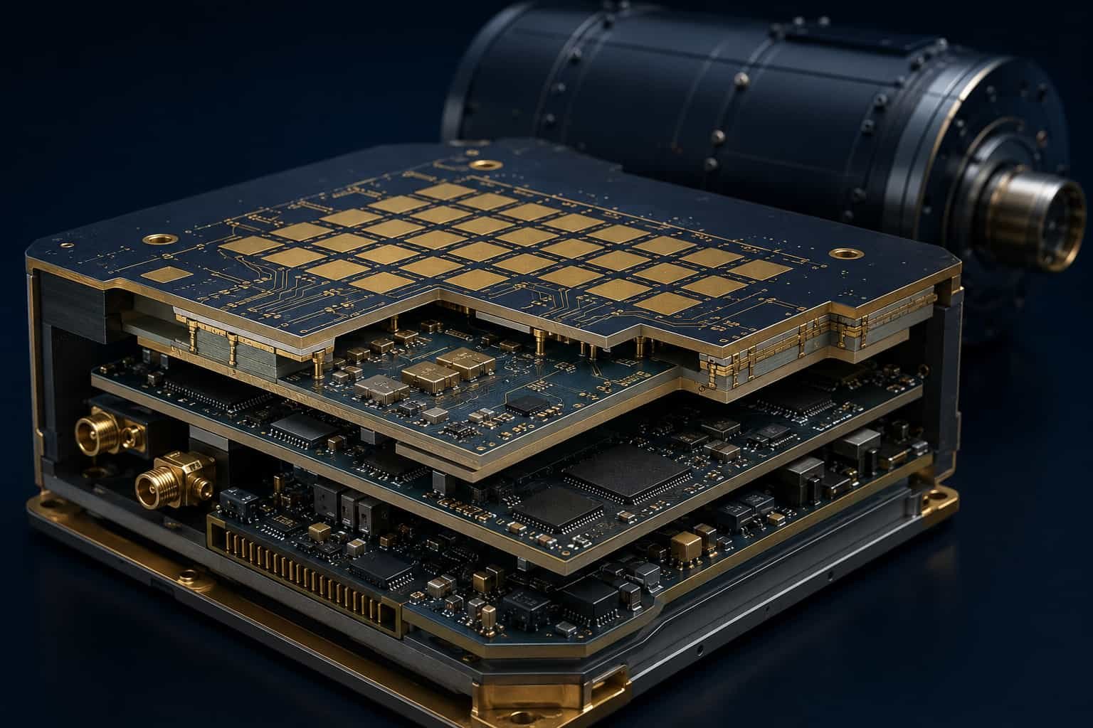
Quick Summary
Key point: Missile seeker PCB typically uses Rogers RO3003 (Dk 3.0, Df 0.0010) for X-band and Ka-band seekers, and Rogers RT5880 (Dk 2.2, Df 0.0009) for the lowest-loss Ka-band and W-band applications. Key manufacturing challenges are compact multilayer design within cylindrical volume constraints, high-g shock survival (500–20,000 g depending on platform), wide temperature range from -55°C to +125°C or beyond, and IPC Class 3 workmanship with full material traceability. Single-use mission profile means zero in-service repair — every board must be right before integration.
Missile guidance PCB occupies a unique position in the high frequency PCB spectrum. It combines the material and frequency requirements of the most demanding radar PCB with the environmental qualification requirements of space-borne electronics — and adds high-g shock loading that neither radar nor space PCB typically faces. This combination makes missile seeker PCB one of the most technically demanding products in defense electronics manufacturing.
Missile Seeker Types and High Frequency PCB Requirements
Missile seekers use different guidance methods, each with different frequency and PCB requirements. Understanding the seeker type is the starting point for correct PCB specification.
Active Radar Homing (ARH)
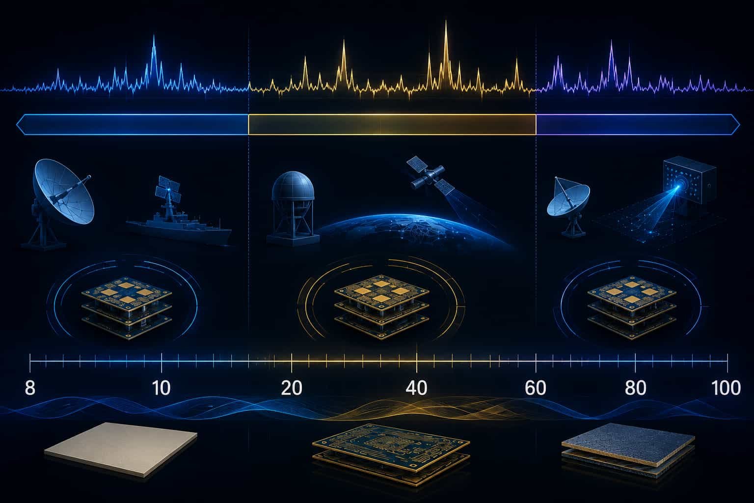
Active radar homing seekers carry their own radar transmitter and receiver. The seeker illuminates the target and receives the reflected signal to guide the missile. This is the most common type for modern precision-guided missiles. Operating frequencies range from X-band for longer-range missiles to Ka-band and W-band for highly miniaturized seekers.
- X-band ARH (8–12 GHz): Rogers RO3003 or RO4003C — most common for medium-range ARH missiles
- Ka-band ARH (26.5–40 GHz): Rogers RO3003 — lowest loss and best Dk stability at Ka-band
- W-band ARH (75–110 GHz): Rogers RT5880 — only viable standard material at W-band
- PCB size: constrained by seeker diameter — typically 60–200 mm circular board
- Requires RF transmit chain, receive chain, local oscillator, and signal processor in minimum volume
Semi-Active Radar Homing (SARH)
Semi-active radar homing seekers receive radar energy reflected from the target, which is illuminated by a separate radar on the launch platform. The missile carries only a receiver, not a transmitter, which simplifies the seeker PCB.
- Frequency: matched to the illuminating radar — X-band most common
- PCB: receive-only — lower RF power handling requirement than ARH
- Rogers RO3003 or RO4003C for X-band SARH seeker receiver PCB
- Smaller and lighter than ARH seeker PCB due to absence of transmit chain
Millimeter-Wave (MMW) Seeker
Millimeter-wave seekers operating at Ka-band or W-band offer higher resolution target discrimination and better performance in adverse weather compared to lower-frequency seekers. The PCB design at these frequencies requires the most advanced materials and tightest manufacturing tolerances.
- Ka-band (35 GHz): Rogers RO3003 — antenna element size approximately 4 mm, tight manufacturing tolerances
- W-band (94 GHz): Rogers RT5880 — antenna element size approximately 1.6 mm, minimum line width 2.5 mil or below
- Compact array: small seeker diameter means fewer antenna elements — array design must maximize gain within volume constraint
- Dual-mode seekers: may combine MMW radar with IR or laser — PCB must support multiple sensor modalities
Anti-Radiation Missile (ARM) Seeker
Anti-radiation missile seekers home on the radar emissions of the target. They must cover a wide frequency range to detect and track different radar types, placing requirements on the PCB similar to those of EW receivers — wide instantaneous bandwidth and low insertion loss across the full frequency range.
- Frequency coverage: typically 2–18 GHz or wider — must cover multiple radar band threats
- Rogers RT5880 preferred — lowest and most stable Dk across wide frequency range
- Passive receive only — no transmitter PCB required
- High sensitivity: minimum insertion loss in receive chain critical for long detection range
Rogers PCB Material Selection for Missile Seeker
Material selection for missile seeker PCB is driven by operating frequency, insertion loss budget, size and weight constraints, and the extreme environmental qualification requirements of the missile platform.
Rogers RO3003 — Standard for Ka-Band and Below
Rogers RO3003 is the most widely used material for missile seeker PCB operating at X-band through Ka-band. Its combination of Dk 3.0, Df 0.0010, low CTE (x-y 17 ppm/°C), PTFE base (no Tg concern), and availability in thin substrates (0.127 mm) makes it the best-suited standard material for compact high-frequency seeker designs.
- Dk: 3.0 ±0.04 — tight tolerance critical for consistent antenna resonance in production
- Df: 0.0010 — very low loss across X-band to Ka-band
- x-y CTE: 17 ppm/°C — closely matches copper, good for compact PCB with thermal cycling
- z-axis CTE: 24 ppm/°C — lower than RT5880, better via fatigue life in high-g and thermal cycling
- Minimum thickness: 0.127 mm — supports very thin dielectric layers for Ka-band antenna feed structures
- Applications: X-band ARH seekers, Ka-band MMW seekers, SARH receiver PCB
Rogers RT5880 — For W-Band and Ultra-Low Loss
Rogers RT5880 is used for W-band seeker applications and any Ka-band design requiring the absolute minimum insertion loss. Its Dk of 2.2 and Df of 0.0009 are the lowest of standard PCB materials, but its higher z-axis CTE (237 ppm/°C) requires more careful via design for high-g shock and thermal cycling.
- Dk: 2.2 ±0.02 — lowest standard seeker PCB material
- Df: 0.0009 — minimum loss at W-band and Ka-band
- z-axis CTE: 237 ppm/°C — very high, critical consideration for high-g shock via reliability
- Minimum thickness: 0.127 mm — available for compact Ka-band and W-band designs
- Applications: W-band ARH seekers, Ka-band ARM seekers requiring minimum loss
Design guidance: For Ka-band seeker PCB where both performance and via reliability are important — particularly for high-g gun-launched or rocket-boosted platforms — Rogers RO3003 is generally preferred over RT5880 because its lower z-axis CTE (24 vs 237 ppm/°C) provides significantly better via barrel fatigue resistance under the repeated high-g and thermal stress of the missile environment.
Miniaturization and Compact Design for Missile Seeker PCB
Missile seeker PCB must fit within the physical constraints of the seeker head — typically a circular cross-section with diameter ranging from 60 mm for small tactical missiles to 200 mm or more for larger systems. This constraint drives aggressive miniaturization of the RF circuits, antenna array, and signal processing electronics.
Circular PCB and Conformal Designs
Many missile seeker PCB designs use circular boards that fit within the cylindrical seeker housing. Circular PCB design places constraints on trace routing, component placement, and via structure that do not exist in rectangular designs.
- Circular board diameter: 60–200 mm depending on missile class
- Component placement: all circuits must fit within the circle — corner areas unavailable
- RF traces: must route from antenna elements at the periphery to the central RF chip package
- Ground plane: must be continuous and uninterrupted under the antenna aperture — difficult in circular designs
- Stacking: multiple boards stacked axially within the seeker housing — thin boards preferred
Minimum Line Width at Ka-Band and W-Band
At Ka-band and W-band, antenna element dimensions and feed line widths are small enough that they approach the manufacturing minimum line width capability. This makes the choice of manufacturer critical for Ka-band and W-band seeker PCB.
- 50Ω microstrip on RO3003 0.254 mm at 35 GHz: trace width approximately 0.6 mm (24 mil)
- 50Ω microstrip on RO3003 0.127 mm at 35 GHz: trace width approximately 0.3 mm (12 mil)
- Antenna element at 35 GHz on RO3003 0.254 mm: approximately 3.5–4.0 mm
- 50Ω microstrip on RT5880 0.127 mm at 94 GHz: trace width approximately 0.3 mm (12 mil)
- Antenna element at 94 GHz on RT5880 0.127 mm: approximately 1.3–1.5 mm
- Minimum manufacturing line width required: 2.5 mil for Ka-band, 2.5 mil or below for W-band
High Density Interconnect for Compact Seeker PCB
To route all seeker electronics — RF front-end, signal processing, power management, and telemetry — within the constrained volume of a missile seeker, HDI design with blind and buried vias is commonly used. This increases routing density without increasing board diameter.
- HDI: 1-stage or 2-stage blind vias for Ka-band seeker PCB
- Layer count: typically 8–16 layers for a complete ARH seeker PCB
- Minimum via diameter: 0.1–0.15 mm for laser blind vias in thin PTFE substrates
- PTFE lamination limit: maximum 2 press cycles — limits HDI stage count
For blind and buried via capabilities in high frequency PCB, see Blind and Buried Via Capabilities in High Frequency PCB Manufacturing. For multilayer stackup design, see Multilayer High Frequency PCB: Layer Count, Stackup and Manufacturing Limits.
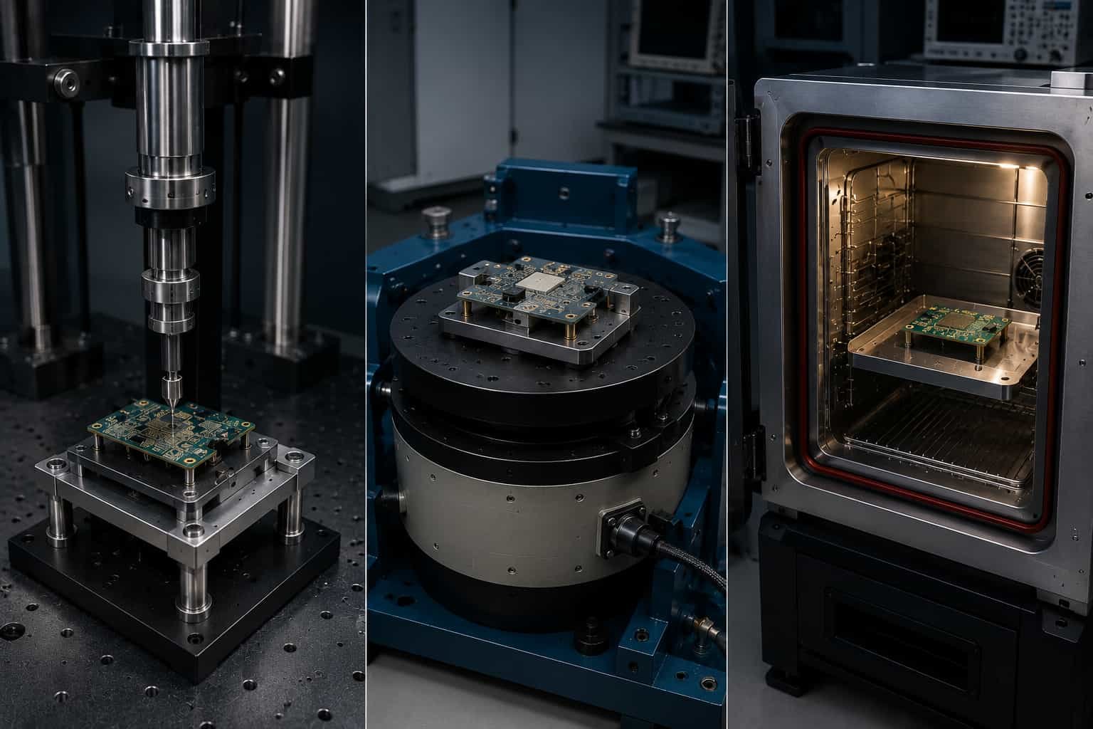
High-g Shock and Vibration Qualification for Missile PCB
The most distinctive environmental requirement of missile seeker PCB — compared to other aerospace and defense PCB — is the high-g shock loading experienced during launch, motor ignition, and in some cases, gun launch. This places unique demands on the PCB via structure, component attachment, and solder joint design.
Launch and Gun-Launch Shock Levels
- Air-launched missile ignition: typically 50–500 g, 10–20 ms duration
- Ground-launched rocket motor: typically 100–1000 g at ignition
- Gun-launched projectile: 10,000–50,000 g during barrel travel — extreme shock loading
- Separation shock: pyrotechnic stage separation creates short-duration high-g shock
- MIL-STD-810 Method 516.8: shock testing standard for military equipment
PCB Design for High-g Shock Survival
PCB via barrels experience tensile and compressive stress during high-g shock loading proportional to the component mass and the board’s response to the shock pulse. For gun-launched systems, the shock levels are high enough to require specialized via design and component attachment methods.
- Via copper plating: IPC Class 3 minimum 25 µm — more ductile than thinner plating, better shock resistance
- Via barrel aspect ratio: lower aspect ratio (shorter barrels relative to diameter) improves shock survival
- Copper-filled vias: eliminate void inside the via barrel, significantly improve shock resistance
- Underfill: applied under heavy components (chips, connectors) to distribute shock load across the component footprint
- Potting: seeker PCB often fully potted in epoxy within the housing — reduces relative motion between components
- Component height: minimize component height to reduce bending moment during shock loading
- Lead-free solder: generally less ductile than tin-lead — shock resistance of solder joints must be verified
Vibration
Rocket motor burn vibration is sustained throughout the powered phase of flight. The PCB must survive the vibration power spectral density (PSD) levels specified for the missile platform across the full burn duration.
- Typical rocket motor vibration: 0.04–0.1 g²/Hz from 20–2000 Hz during motor burn
- PCB natural frequency: should be above 2000 Hz to avoid resonance in the motor burn vibration range
- Heavy components: require additional attachment support at high vibration levels
- Conformal coating: helps retain component leads and solder joints under vibration
- MIL-STD-810 Method 514.8: vibration testing for military equipment
Thermal Requirements for Missile Seeker PCB
Missile seeker PCB faces thermal requirements at both ends of the temperature spectrum. Cold storage and transport may reach -55°C or colder. During high-speed flight, aerodynamic heating of the seeker dome and housing can raise internal temperatures significantly above ambient. GaN radar transmitter chips add high local power dissipation to the thermal budget.
Storage and Operating Temperature Range
- Storage temperature: typically -55°C to +71°C for standard military missiles
- Operating temperature: -40°C to +85°C for most missile seeker electronics during flight
- Aerodynamic heating: high-speed missiles may see internal temperatures above +125°C — depends on Mach number and flight duration
- Rogers RO3003 and RT5880: PTFE base, no Tg concern across any missile temperature range
- Thermal cycling: temperature cycling qualification from storage minimum to operating maximum — typically 100–500 cycles
GaN Transmitter Thermal Management
Active radar homing seeker transmitters using GaN MMIC chips dissipate significant RF power in a very small PCB area. Thermal management of the GaN chip is critical for both reliability and performance — junction temperature must remain within specification throughout the transmit pulse.
- GaN seeker transmitter power dissipation: typically 2–10W in a compact chip package
- Thermal via array: 0.2–0.3 mm diameter, 0.4–0.6 mm pitch under GaN package
- Copper coin insert: for highest-power GaN chips where standard via array thermal resistance is insufficient
- Rogers RO3003 thermal conductivity: 0.50 W/m·K — 2.5× higher than RT5880 — preferred for highest-power transmitters
- Heat path: chip → thermal vias → copper spreader plane → PCB edge → housing → external fin or airframe
IPC Class 3 and Quality Requirements for Missile Seeker PCB
Missile seeker PCB requires IPC Class 3 workmanship as the manufacturing baseline. Many missile programs impose additional requirements above Class 3, particularly for via copper plating, microsection frequency, and traceability documentation.
- PTH copper plating: IPC Class 3 minimum 25 µm average, 20 µm minimum — missile programs often specify 30 µm or higher
- No annular ring breakout on any layer — critical for compact Ka-band seeker designs with tight pad rings
- Void maximum: 5% of hole length per Class 3 — some programs specify no voids
- 100% electrical test: continuity and isolation for every board
- Microsection FAI: required, plus periodic lot sampling — some programs require microsection every lot
- Copper-filled blind vias: required for stacked blind vias and recommended for all blind vias in high-g applications
- Material certificates: Rogers CoC with lot number — ZY or other alternatives typically not acceptable
- Serialization: every board or assembly carries a unique serial number traceable to all process records
- MIL-PRF-31032: US military PCB specification applicable to many missile seeker PCB programs
For IPC Class 3 requirements in detail, see IPC Class 3 High Frequency PCB: What It Means for Aerospace and Defense Applications. For wide temperature range material requirements, see Wide Temperature Range PCB: Material and Manufacturing for Aerospace Applications.
Single-Use Mission Profile and Its Impact on PCB Specification
Unlike aircraft avionics or ground-based radar that must be maintained and repaired over decades of service, a missile seeker PCB has a single-use mission profile. Once the missile is fired, the seeker electronics must function correctly for the duration of the engagement — typically seconds to minutes — and then the mission is complete.
Implications for PCB Specification
The single-use nature of missile seeker PCB changes some specification priorities compared to long-service-life systems:
- Solder joint lifetime: only needs to survive from storage through the single flight — not years of thermal cycling in service
- Via fatigue: must survive storage, transport, launch shock, and flight — not long-term in-service thermal cycling
- Component reliability: screening and burn-in to eliminate early failures is important — in-service wearout is not the concern
- Cost: per-unit PCB cost is less sensitive for low-volume precision weapons — performance and reliability are the priorities
- Qualification: extensive environmental qualification upfront — no in-service verification possible
Pre-Launch Qualification vs. In-Service Monitoring
- All qualification testing is done before production release — no in-service data
- Environmental qualification: shock, vibration, thermal cycling, humidity, altitude — all done on qualification units
- Accelerated life testing: must demonstrate that stored missiles will function when needed after years of storage
- Storage life: missiles may be stored for 10–20 years before use — PCB and components must maintain readiness
- Periodic readiness testing: some programs test a sample of stored missiles periodically to verify storage life
Information Needed for Missile Guidance and Seeker PCB Quotation
To review feasibility and provide an accurate quotation for missile seeker high frequency PCB, the following information should be prepared:
- Gerber files (all layers) and NC drill files
- Complete PCB stackup with Rogers material grade, layer sequence, and dielectric thickness
- Seeker type — ARH, SARH, MMW, ARM, or other
- Operating frequency band — X-band, Ka-band, W-band, or wideband
- PCB form factor — circular diameter or rectangular dimensions
- Layer count and minimum board thickness
- Via structure — through-hole, blind, buried, copper-filled vias
- Controlled impedance requirements — target, tolerance
- High-g shock requirement — peak g-level, duration, axis
- Vibration requirement — PSD level and frequency range
- Temperature range — storage and operating
- Thermal requirements — RF chip power dissipation
- IPC Class requirement and any requirements above Class 3
- Applicable standards — MIL-PRF-31032, MIL-STD-810, MIL-STD-461, or other
- Traceability requirements — Rogers CoC, serialization, record retention
- Surface finish and thickness specification
- Quantity — engineering development, qualification, or production
For a complete file checklist, see What Files Are Needed for a High Frequency PCB Quotation?. For radar system PCB requirements, see High Frequency PCB for Radar Systems: EW, AESA and Ground-Based Radar.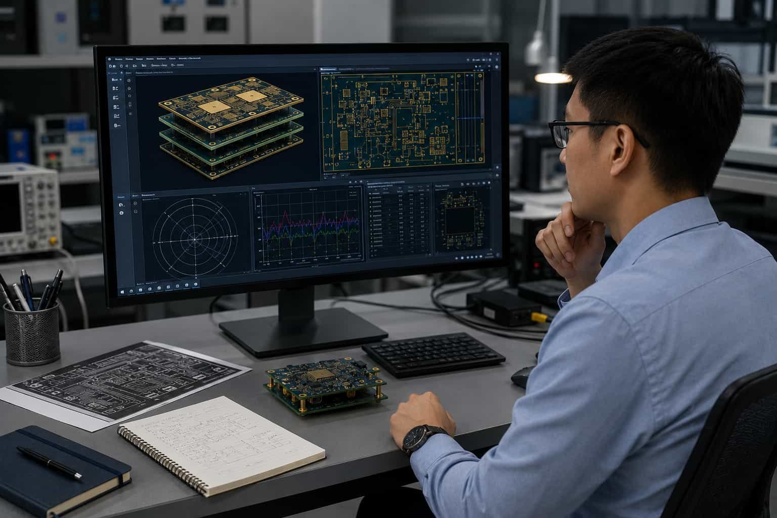
Conclusion
Missile guidance and seeker PCB represents the highest combined demand for high frequency performance, environmental robustness, miniaturization, and manufacturing quality in defense electronics. Rogers RO3003 is the standard material for X-band through Ka-band ARH seekers, offering the best combination of low Df, CTE compatibility with copper, and PTFE-base thermal stability. Rogers RT5880 is used for W-band seekers and the lowest-loss Ka-band applications, with careful attention to via design for high-g shock survival.
IPC Class 3 workmanship, Rogers-certified material documentation, copper-filled vias for high-g reliability, high-density multilayer design within cylindrical volume constraints, and qualification to MIL-STD-810 shock and vibration standards are the framework for high frequency PCB in missile guidance and seeker applications. Early engagement with a manufacturer experienced in the specific combination of PTFE materials, compact Ka-band design, and defense qualification requirements is essential for successful development and production.