PTFE PCB Plasma Activation: Why It Must Be In-House and How It Works

The chemistry behind plasma activation, the critical 2-hour window between activation and plating, why outsourcing fails, and how to verify your factory actually performs it correctly.

Table of Contents

Key point: Most factories quote 3–4 weeks waiting for RO3003 / RT5880 material procurement. Riching PCB maintains these materials in stock — no material wait.

PTFE PCB requires plasma or sodium naphthalene hole wall activation before copper plating — performed in-house, within 2–4 hours before copper plating starts. Outsourced plasma activation fails because the activated surface deactivates within hours of air exposure. Boards without proper plasma activation pass all initial electrical tests and fail after 3–5 thermal cycles. The fastest verification: ask for RO3003 prototype lead time — 7–10 days means in-house capability; 5–7 days (same as FR4) means no plasma activation.

Plasma activation is the single process step that separates a capable PTFE PCB manufacturer from a factory that will produce boards that fail in the field. Every PTFE material — Rogers RO3003, RT5880, RT5870, Taconic TLY-5, RF-35, F4B series — requires plasma or sodium naphthalene hole wall activation before copper plating. Without it, copper deposits on the PTFE surface with zero mechanical adhesion.

This guide explains the chemistry of plasma activation, why the 2-hour window between activation and plating is non-negotiable, what happens to boards made without it, and how to verify your factory actually performs this process in-house.

Why PTFE Cannot Be Plated Without Activation

PTFE (polytetrafluoroethylene) is one of the most chemically inert materials in commercial use. Its carbon-fluorine bonds are among the strongest in organic chemistry — this is why PTFE is non-stick, chemically resistant, and stable at extreme temperatures. It is also why copper cannot bond to it.

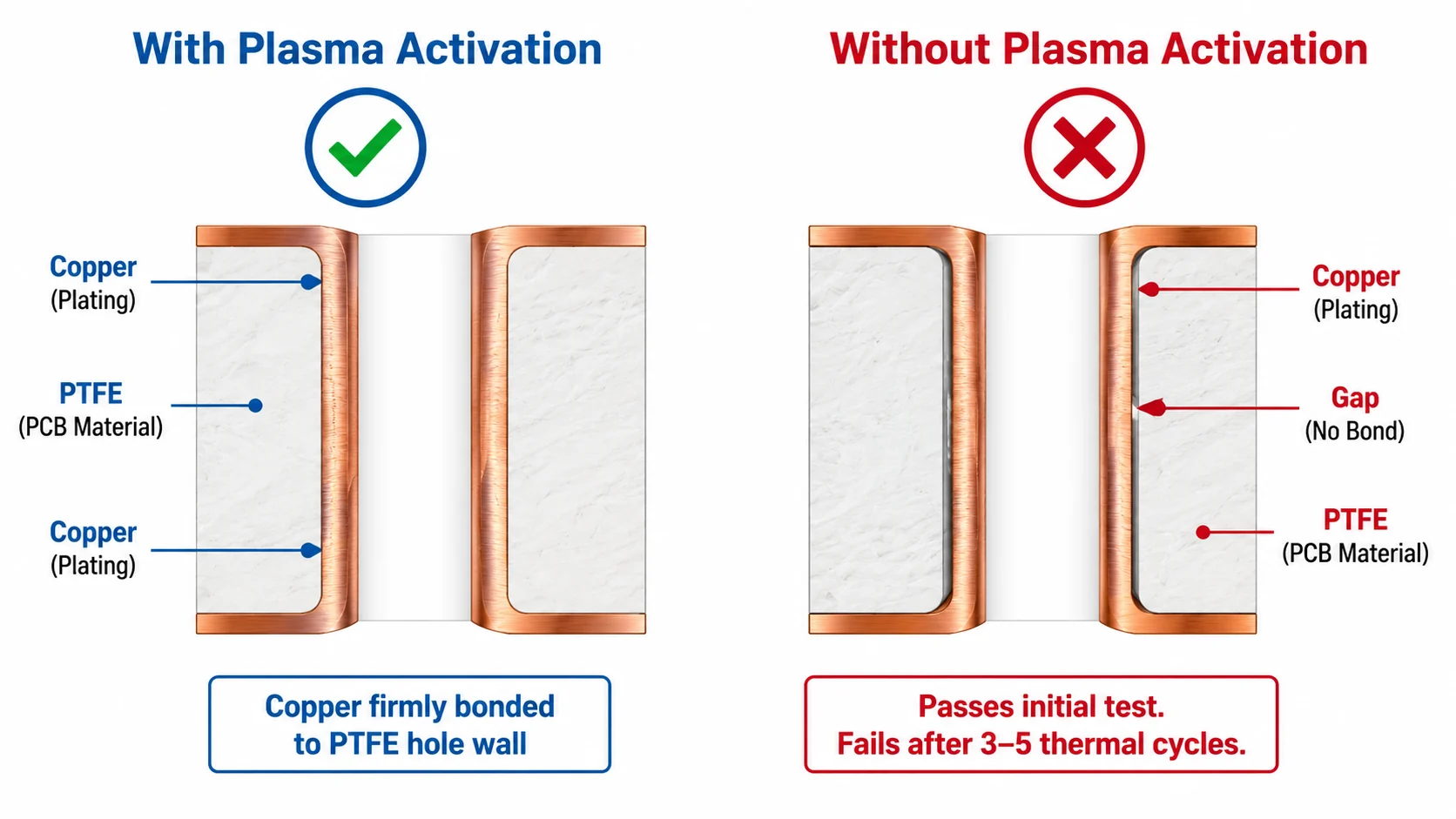
When a drill passes through PTFE laminate, the hole wall is a smooth, chemically inert PTFE surface. Electroless copper requires a surface with micro-roughness and chemical anchor points to nucleate and adhere. On untreated PTFE, the copper layer deposits as a film with no mechanical adhesion — it appears continuous under optical inspection but separates from the hole wall under the stress of thermal cycling.

Plasma activation solves this by bombarding the PTFE surface with ionized gas (typically oxygen, argon, or a mixture). The high-energy ions break carbon-fluorine bonds at the surface, creating free radicals, polar groups, and micro-roughness that allow electroless copper to mechanically anchor to the PTFE. The surface is now chemically active — but only temporarily.

The 2-Hour WindowPTFE PCB plasma activation process timeline showing the critical 2-hour window between activation and copper plating

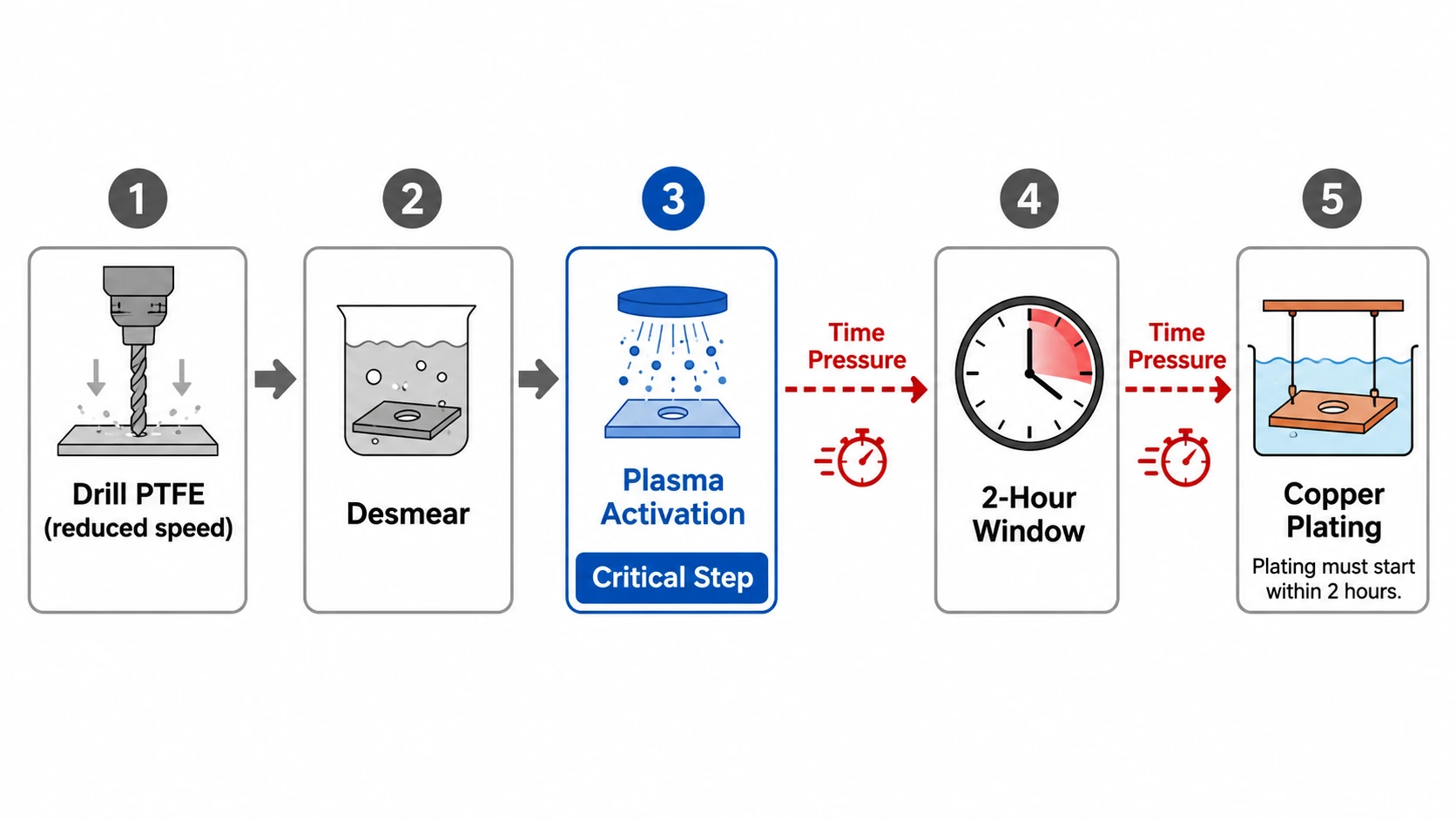
Plasma-activated PTFE surfaces begin to lose their activated state immediately upon exposure to air. Free radicals recombine, polar groups degrade, and surface energy decreases. The rate of deactivation depends on temperature, humidity, and ambient contamination — but under typical factory conditions, a plasma-activated PTFE surface loses most of its adhesion-enabling chemistry within 2–4 hours.

This is the fundamental reason why plasma activation must be performed in-house and why outsourcing it fails:

  • In-house: activation and plating performed in the same facility, same shift — 1–2 hours between steps
  • Outsourced: activated boards packaged, transported to plating facility, unpackaged — minimum 4–8 hours, often 24+ hours
  • Result of outsourcing: copper plating begins on a surface that has already largely deactivated — adhesion is inconsistent, ranging from marginal to zero

Boards with outsourced plasma activation will typically pass initial electrical continuity testing — the copper layer is present and continuous. They fail after 3–5 thermal cycles when the copper separates from the PTFE hole wall.

What Happens Without Plasma ActivationPTFE PCB failure diagram showing copper delamination from hole wall without plasma activation after thermal cycling

Failure ModeRoot CauseWhen It Appears
Copper separates from hole wallNo plasma — PTFE is chemically inertAfter 3–5 thermal cycles –40°C to +85°C
Intermittent via opensPartial copper delamination under stressDuring thermal shock or vibration
Passes initial continuity testCopper layer present but not bondedPasses at delivery — fails in field
Marginal adhesion with outsourced plasmaSurface deactivated during transportInconsistent lot-to-lot reliability
Cannot be detected or repairedFailure is in hole wall, not surfaceField return after deployment

Plasma vs Sodium Naphthalene: Two Valid Methods

RF Plasma Activation

Plasma activation uses radio-frequency ionized gas (typically oxygen plasma or argon/oxygen mixture) to modify the PTFE surface. The process takes 10–30 minutes per batch in a vacuum chamber. Plasma activation is cleaner, more controllable, and more consistent than chemical methods. It is the standard process at most capable PTFE PCB manufacturers including Riching PCB.

Sodium Naphthalene Treatment

Sodium naphthalene (also called sodium naphthalenide) is a chemical etchant that reacts with PTFE to defluorinate the surface, creating carbon-rich micro-roughness. It is an older method, effective but more hazardous to handle. Some manufacturers use it as an alternative to plasma — it is equally valid if performed correctly, in-house, immediately before plating. The same 2-hour window applies.

The PTFE PCB Plasma Activation Process

StepProcessCritical Requirement
1. DrillingMechanical drill at reduced PTFE-specific spindle speedStandard FR4 speed causes PTFE smear — prevents adhesion even after activation
2. DesmearRemove drill debris from hole wallMust be performed before activation
3. Plasma activationRF plasma or sodium naphthalene treatmentMust be in-house — 2–4 hour window to plating
4. Copper platingElectroless copper + electrolytic platingMust start within 2–4 hours of activation
5. Pattern imagingInner or outer layer etchingStandard process after plating
6. LaminationPress cycle for multi-layer stackupMaximum 2 press cycles for all PTFE materials

How to Verify Your Factory Performs Plasma Activation In-House

QuestionIn-House Factory AnswerRed Flag
Is plasma activation in-house?✅ Yes — our own equipment, every order🚩 Outsourced / partner does it
How long after activation to plating?✅ 2–4 hours, same shift🚩 No specific answer
What PTFE grades do you stock?✅ RO3003, RT5880 — in stock, no wait🚩 We can source any material
Lead time for RO3003 prototype?✅ 7–10 working days🚩 5–7 days (same as FR4)
Drill parameters for PTFE?✅ Reduced spindle speed, PTFE-specific🚩 Same as FR4
Max lamination cycles for PTFE?✅ Maximum 2 cycles🚩 No limit stated

The single fastest verification is the lead time test: ask for RO3003 prototype lead time. A factory with in-house plasma activation quotes 7–10 working days. A factory without it quotes 5–7 days — physically impossible if plasma activation is being performed correctly within the manufacturing sequence.

Which PTFE Materials Require Plasma Activation

  • Rogers RO3003(Dk 3.0, Df 0.0010) — PTFE ceramic
  • Rogers RT5880(Dk 2.20, Df 0.0009) — PTFE glass
  • Rogers RT5870 (Dk 2.33, Df 0.0012) — PTFE glass
  • Rogers RO3006 (Dk 6.15) — PTFE ceramic
  • Rogers RO3010 (Dk 10.2) — PTFE ceramic
  • Rogers RO6010 (Dk 10.2) — ceramic PTFE
  • Taconic TLY-5, TLP-5, TLY-3 — PTFE glass
  • Taconic RF-35, RF-60A, CER-10 — PTFE
  • F4BM220, F4BM255, F4BTM series — PTFE


Rogers RO4350B and RO4003C (hydrocarbon ceramic) do NOT require plasma activation — they use standard FR4-compatible process. See RO4350B vs RO3003 for the full process difference between hydrocarbon and PTFE Rogers materials.

Riching PCB Plasma Activation Process

  • Equipment: in-house RF plasma chamber — not outsourced
  • Timing: activation and copper plating performed same day, same shift
  • Materials: RO3003, RT5880, RT5870, Taconic TLY-5, RF-35, F4B series — all in stock
  • Stock availability: no material procurement wait — 7–10 working day prototype
  • Verification: TDR impedance on every lot, material Dk certificate available on request

Conclusion

PTFE PCB plasma activation must be performed in-house, immediately before copper plating, within a 2–4 hour window. Outsourced plasma activation produces boards that pass initial testing and fail in the field. The fastest way to verify in-house capability is the lead time test: RO3003 prototype should quote 7–10 days. Riching PCB performs plasma activation in-house on all PTFE orders — RO3003, RT5880, Taconic and F4B in stock, no material wait, 7–10 day prototype. See PTFE PCB manufacturing challenges overview for the complete manufacturing guide.

Order PTFE PCB with In-House Plasma Activation

RO3003, RT5880, Taconic, F4B — in stock, no material wait. Plasma activation in-house every order. Send the following:

  • Gerber files + NC drill file
  • PTFE material grade and dielectric thickness
  • Stackup drawing — copper weight per layer
  • Controlled impedance requirements
  • IPC Class and quantity

WhatsApp +86 13760473650— 7–10 day prototype, no material wait

Q&A

PTFE PCB Plasma Activation Q&A

Common questions about why plasma activation is required, the 2-hour window, how to verify factory capability, and which Rogers materials need activation.

Why does PTFE PCB require plasma activation?

PTFE is chemically inert — carbon-fluorine bonds prevent copper from bonding. Plasma breaks these bonds at the hole wall surface, creating micro-roughness for copper to anchor. Without it, copper deposits with zero adhesion and separates after 3–5 thermal cycles.

Why must plasma activation be in-house?

The window between activation and plating must be 2–4 hours. Outsourcing requires transport — minimum 4–8 hours, often 24+. By the time plating starts, the surface has deactivated. In-house means activation and plating in the same facility, same shift.

How do I verify a factory performs plasma activation in-house?

Ask for RO3003 prototype lead time. In-house: 7–10 working days. Without it: 5–7 days (same as FR4) — physically impossible if plasma is done correctly. Also ask: is plasma equipment on-site? How long between activation and plating? A capable factory gives specific answers.

What is the difference between plasma and sodium naphthalene treatment?

Both valid. Plasma: ionized gas, cleaner and more controllable. Sodium naphthalene: chemical etchant, older but effective. Both must be in-house, immediately before plating. Same 2–4 hour window applies to both.

Which Rogers materials require plasma activation?

All PTFE-based Rogers: RO3003, RT5880, RT5870, RO3006, RO3010, RO6010. Rogers RO4350B and RO4003C are hydrocarbon ceramic — NO plasma required, standard FR4-compatible process.

PCB Project Review

Request a PCB Quote

Upload your Gerber ZIP file and project requirements. Our engineering team will review your PCB material, stackup, impedance needs, surface finish, and production quantity before quoting.

Please prepare:

  • Gerber files in ZIP format
  • PCB material or stackup requirements
  • Controlled impedance notes if available
  • Prototype or batch production quantity
ZIP format only. Please compress all Gerber and drill files into one ZIP package before uploading.