RO4350B vs RO4003C: Insertion Loss, Cost and Manufacturing Differences
Rogers RO4350B and RO4003C use the same FR4-compatible manufacturing process — the only difference is Df (0.0037 vs 0.0027) and available thicknesses. Here is when the lower loss justifies the higher cost.
Home » high frequency PCB material » RO4350B vs RO4003C: Insertion Loss, Cost and Manufacturing Differences
Table of Contents
Key point: RO4350B (Df 0.0037) and RO4003C (Df 0.0027) use identical FR4-compatible manufacturing — same process, same lead time, same drill parameters, no plasma activation required. The only difference is Df: RO4003C is 27% lower. At 1 GHz the insertion loss difference is negligible (~0.05 dB/cm). At 10 GHz it is ~0.15 dB/cm; at 18 GHz ~0.25 dB/cm. RO4003C is worth the 20–30% material cost premium for X-band (8–12 GHz) and Ku-band (12–18 GHz) designs with long traces or tight loss budgets. For designs below 6 GHz, RO4350B provides better cost-performance. Neither material is suitable above 20 GHz — PTFE (RO3003, RT5880) required.
Rogers RO4350B and RO4003C are both hydrocarbon ceramic laminates from the RO4000 series. They share the same FR4-compatible manufacturing process — no plasma activation, same drill parameters, same press cycle, same bondply options. The difference is Df: RO4350B is 0.0037, RO4003C is 0.0027. That 27% reduction in dissipation factor is the only technical reason to choose RO4003C over RO4350B. The question is whether your application actually needs it.
Properties Comparison
| Parameter | RO4350B | RO4003C |
|---|---|---|
| Dielectric Constant (Dk) | 3.48 ± 0.05 | 3.38 ± 0.05 |
| Dissipation Factor (Df) | 0.0037 | 0.0027 ✅ lower |
| Thermal Coeff. of Dk (TCDk) | +50 ppm/°C | +40 ppm/°C |
| Thermal Conductivity | 0.69 W/m/K | 0.64 W/m/K |
| Tg | >280°C | >280°C |
| Process Type | FR4-compatible | FR4-compatible |
| Plasma Activation | Not required | Not required |
| Available Thicknesses (mm) | 0.101 / 0.168 / 0.254 / 0.338 / 0.422 / 0.508 / 0.762 / 1.524 | 0.203 / 0.305 / 0.406 / 0.508 / 0.813 / 1.524 |
| Relative Material Cost | Base | ~20–30% higher |
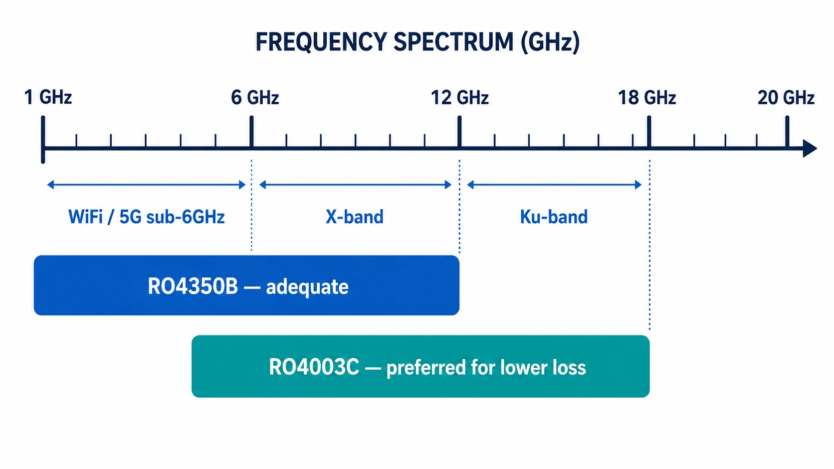
The Key Difference: Df 0.0037 vs 0.0027
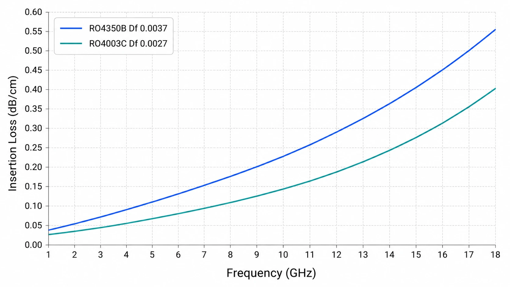
At 1 GHz, the insertion loss difference between RO4350B and RO4003C is approximately 0.05 dB/cm — negligible for any practical design. At 10 GHz, the difference grows to approximately 0.15 dB/cm. Over a 10 cm trace, this represents 1.5 dB — meaningful for tight link budgets but within tolerance for most designs.
At 18 GHz (upper Ku-band), the difference is approximately 0.25 dB/cm. Over a 10 cm trace: 2.5 dB. At this point, choosing RO4003C over RO4350B recovers a significant portion of the insertion loss budget — particularly important for satellite Ku-band terminal PCB where the antenna feed network may span 15–20 cm.
The crossover point where RO4003C becomes clearly worth the cost premium is approximately 8–10 GHz for traces longer than 5 cm, or wherever the insertion loss budget is tight enough that 0.15–0.25 dB/cm matters.
Manufacturing: Identical Process
This is the most important practical point: RO4350B and RO4003C use exactly the same manufacturing process. Same drill parameters, same press cycle, same lamination temperature, same surface finish options. If your factory can manufacture RO4350B, it can manufacture RO4003C with zero process change. There is no plasma activation requirement, no PTFE constraints, no lamination cycle limit difference.
Lead time is identical: 5–7 working days for prototype at Riching PCB. The only difference is material cost — RO4003C is approximately 20–30% more expensive per panel than RO4350B. See Rogers PCB price guide for reference price ranges.
Available Thicknesses
RO4350B thicknesses (mm):
0.101 / 0.168 / 0.254 / 0.338 / 0.422 / 0.508 / 0.762 / 1.524
RO4350B has the widest thickness range of any Rogers material — 8 standard options from 0.101 mm to 1.524 mm. This makes it the most flexible choice for stackup design, particularly for designs requiring thin substrates (0.101 mm, 0.168 mm) at Ka-band or thick substrates (0.762 mm, 1.524 mm) for lower-frequency power amplifier PCB.
RO4003C thicknesses (mm):
0.203 / 0.305 / 0.406 / 0.508 / 0.813 / 1.524
RO4003C has fewer standard thickness options — 6 options starting from 0.203 mm. No 0.101 mm or 0.168 mm option. This means RO4003C cannot be used for designs requiring very thin dielectric (below 0.203 mm), which rules it out for most Ka-band and 5G mmWave antenna designs where 0.127 mm RO3003 is standard.
50Ω Microstrip Trace Width Comparison
Because RO4003C has lower Dk (3.38 vs 3.48), the same impedance requires a slightly wider trace:
- 50Ω microstrip on RO4350B 0.254 mm, 1 oz copper: ~0.56 mm
- 50Ω microstrip on RO4003C 0.305 mm, 1 oz copper: ~0.67 mm
The difference is small — approximately 0.1 mm wider for RO4003C on a comparable thickness. This is within standard etching tolerance and does not affect layout significantly.
Application Selection Guide
| Application | Recommended | Reason |
|---|---|---|
| WiFi 6 / 6E (2.4–6 GHz) | RO4350B | Df 0.0037 adequate, lower cost |
| 5G sub-6GHz (3.3–5.0 GHz) | RO4350B | Df 0.0037 adequate for most designs |
| 5G sub-6GHz tight loss budget | RO4003C | Df 0.0027 reduces insertion loss ~27% |
| X-band radar (8–12 GHz) | RO4003C | Lower Df significant at X-band |
| Ku-band (12–18 GHz) | RO4003C | RO4350B loss becomes marginal above 12 GHz |
| Satellite Ku-band terminal | RO4003C | Insertion loss critical in long feed networks |
| Base station PA PCB (3.5 GHz) | RO4350B | Df adequate, lower material cost |
| Above 20 GHz | RO3003 or RT5880 | Both RO4000 series insufficient above 20 GHz |
When NOT to Use RO4003C
- Designs below 6 GHz where insertion loss budget is comfortable — the 27% Df reduction produces negligible improvement at lower frequencies
- Designs requiring substrate thickness below 0.203 mm — RO4003C is not available in 0.101 mm or 0.168 mm
- Cost-sensitive prototype evaluation — start with RO4350B, upgrade to RO4003C only if insertion loss measurements show it is needed
- Designs above 20 GHz — both RO4350B and RO4003C have Df too high for Ka-band and above. Use Rogers RO3003 (Df 0.0010, PTFE)or RT5880 (Df 0.0009, PTFE)
Summary: Choose RO4003C When
- Operating frequency is above 8 GHz and insertion loss budget is tight
- Ku-band (12–18 GHz) satellite or radar application with long feed networks
- X-band (8–12 GHz) radar where every 0.1 dB matters
- RF trace lengths exceed 5 cm at frequencies above 6 GHz
- Existing design uses RO4350B and post-prototype measurements show borderline insertion loss
Conclusion
RO4350B and RO4003C use the same FR4-compatible manufacturing process with identical lead time and process requirements. RO4003C’s 27% lower Df (0.0027 vs 0.0037) becomes meaningful above 8 GHz for designs with tight insertion loss budgets, particularly Ku-band satellite and X-band radar applications. For designs below 6 GHz or where insertion loss budget is comfortable, RO4350B provides the better cost-performance balance. For designs above 20 GHz, neither material is adequate — see Rogers materials overview for PTFE material options.
Get a Quote — RO4350B or RO4003C
Both grades in stock. Same 5–7 day lead time. Send the following:
- Gerber files + NC drill file
- Material grade (RO4350B or RO4003C) and dielectric thickness
- Stackup — copper weight per layer
- Controlled impedance requirements
- Quantity and IPC Class
WhatsApp +86 13760473650 — quotation within 4–8 hours
RO4350B vs RO4003C Q&A
Common questions about the difference between Rogers RO4350B and RO4003C, when to choose each, manufacturing process and available thicknesses.
What is the difference between RO4350B and RO4003C?
Same FR4-compatible process, same lead time. Only difference: Df — RO4350B 0.0037, RO4003C 0.0027 (27% lower). RO4003C also has slightly lower Dk (3.38 vs 3.48), fewer thickness options, and ~20–30% higher material cost.
When should I choose RO4003C over RO4350B?
Above 8 GHz with tight insertion loss budget; Ku-band (12–18 GHz) satellite or radar; RF traces >5 cm above 6 GHz; or if post-prototype measurements show RO4350B is borderline. Below 6 GHz, RO4350B is better cost-performance. Neither suitable above 20 GHz — use RO3003 or RT5880 PTFE.
Does RO4003C require different manufacturing than RO4350B?
No — exactly the same process. Same drill parameters, same press cycle, no plasma activation. Lead time identical: 5–7 working days. Zero process change required.
What thicknesses are available for RO4003C vs RO4350B?
RO4350B: 8 options from 0.101–1.524 mm. RO4003C: 6 options from 0.203–1.524 mm — no 0.101 mm or 0.168 mm. If you need very thin dielectric below 0.203 mm, only RO4350B is available.
Can I switch from RO4350B to RO4003C mid-project?
Yes, but recalculate trace width — RO4003C Dk 3.38 vs 3.48 produces ~0.05–0.10 mm wider traces for the same impedance. Update layout before switching. Process and lead time identical — no other changes required.
Request a PCB Quote
Upload your Gerber ZIP file and project requirements. Our engineering team will review your PCB material, stackup, impedance needs, surface finish, and production quantity before quoting.
Please prepare:
- Gerber files in ZIP format
- PCB material or stackup requirements
- Controlled impedance notes if available
- Prototype or batch production quantity
