RF Via Fence PCB: Spacing Rules, Applications and Design Guide for Isolation
Ground via fence design rules for RF PCB — the λ/10 spacing limit, drill size and pad recommendations, GCPW via fence requirements, and manufacturing minimum via spacing constraints.
Home » F4B Rogers alternative » RF Via Fence PCB: Spacing Rules, Applications and Design Guide for Isolation
Table of Contents
Key point: Via fence spacing must be ≤ λ/10 at the operating frequency. On RO4350B at 28 GHz: λ/10 ≈ 0.6 mm. At 77 GHz: λ/10 ≈ 0.3 mm (requires laser drill). GCPW requires via fence as a structural requirement — both coplanar ground conductors must connect to the bottom ground plane through vias. Riching PCB supports 0.2 mm minimum mechanical drill and 0.4 mm center-to-center via spacing for dense via fences. Laser blind vias available for 77 GHz designs. RO4350B, RO3003, RT5880 in stock — no material wait, 5–10 day prototype.
A via fence is a row (or double row) of ground vias placed alongside RF transmission lines to improve isolation, suppress surface wave modes, and maintain ground plane continuity. It is one of the most commonly added features in RF PCB layout — and one of the most commonly implemented incorrectly. Too few vias or too widely spaced, and the fence provides little isolation benefit. Too closely spaced, and the vias approach manufacturing drill-to-drill spacing limits.
This guide covers the λ/10 spacing rule, drill size and pad design recommendations, GCPW via fence requirements, microstrip isolation fences, and manufacturing minimum via spacing constraints at Riching PCB.
What a Via Fence Does
In a microstrip RF PCB, the electromagnetic field extends beyond the trace boundaries into the substrate. At microwave frequencies, this field can propagate as substrate modes — parallel plate modes between the signal layer and ground plane, or surface waves along the substrate surface. These modes cause:
- Cross-coupling between adjacent transmission lines — signal leaking from one channel into another
- Ground plane current return path discontinuities — causing impedance variation
- Parallel plate resonances in multi-layer stackups — creating unexpected notches in S-parameters
A via fence stitches the top ground plane to the bottom ground plane at regular intervals, creating a conductive wall that contains the electromagnetic field and prevents surface wave propagation beyond the fence boundary.
The λ/10 Spacing Rule
| Frequency | λ/10 Spacing (in RO4350B) | Recommended Via Pitch | Note |
|---|---|---|---|
| 6 GHz | ~8.5 mm | ≤6 mm | Relaxed — large spacing acceptable |
| 10 GHz | ~5.1 mm | ≤4 mm | Standard RF |
| 18 GHz (Ku-band) | ~2.8 mm | ≤2.5 mm | Tighter spacing needed |
| 28 GHz (Ka-band) | ~1.8 mm | ≤1.5 mm | Dense via fence required |
| 77 GHz | ~0.65 mm | ≤0.6 mm | Approaching min. mechanical drill limit |
| 100 GHz (W-band) | ~0.47 mm | ≤0.4 mm | Laser drill required |
λ/10 calculated in RO4350B (Dk 3.48). Values in RO3003 (Dk 3.0) and RT5880 (Dk 2.20) are slightly larger.
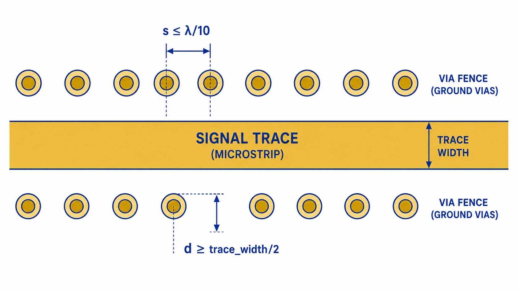
The maximum effective spacing between ground vias in a fence is approximately λ/10 at the operating frequency — where λ is the guided wavelength in the substrate. Beyond λ/10 spacing, the via fence begins to leak electromagnetic energy between vias, reducing isolation effectiveness.
Guided wavelength in a dielectric substrate: λ_g = λ_0 / √(Dk_eff). For RO4350B (Dk 3.48) at 28 GHz: λ_0 = 10.7 mm, Dk_eff ≈ 3.2 (microstrip), λ_g ≈ 6.0 mm, λ/10 ≈ 0.6 mm. This means at Ka-band, ground vias must be spaced no more than 0.6 mm apart — approaching standard mechanical drill minimum spacing limits of 0.4–0.5 mm.
The λ/10 rule is a guideline, not a hard limit. For moderate isolation requirements (20–30 dB), λ/8 spacing is often acceptable. For high isolation (>40 dB), tighter than λ/10 is needed.
Via Fence Design Parameters
Via Drill Diameter
For most RF PCB via fences, 0.3–0.5 mm drill diameter is standard. Smaller vias (0.2–0.3 mm) allow tighter spacing at mmWave frequencies but require more careful DFM review — check fabricator’s minimum drill size and minimum via-to-via spacing (center-to-center and edge-to-edge). At Ka-band and above, 0.2 mm laser-drilled blind vias are sometimes used to achieve the required spacing without going below mechanical drill limits.
Via Pad Diameter
Standard annular ring for via pads: fabricator minimum ring + drill diameter. A 0.3 mm drill with 0.2 mm annular ring gives a 0.7 mm pad diameter. For dense via fences at Ka-band, smaller pads reduce the effective copper obstruction in the ground layer — but must remain above the fabricator’s minimum annular ring specification.
Distance from RF Trace
The first row of via fence vias should be placed at a distance of at least trace_width/2 + clearance from the signal trace edge. A practical rule: keep the inner edge of the via pad at ≥ 1× trace width from the trace edge. Placing vias too close to the signal trace can create capacitive coupling that affects impedance.
Single Row vs Double Row
A single row of vias provides useful isolation — typically 15–25 dB improvement at the design frequency. A double row (two parallel rows of staggered vias) provides 5–10 dB additional isolation. For high-isolation requirements (>40 dB) or mmWave designs where surface wave suppression is critical, double-row via fence is standard.
GCPW Via Fence
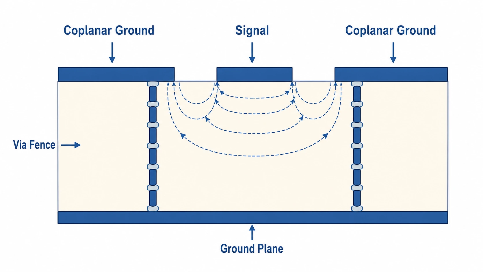
Grounded coplanar waveguide (GCPW) requires via fence as a fundamental structural element — not just an isolation enhancement. In GCPW, the coplanar ground conductors on the top surface must be connected to the bottom ground plane through vias to suppress the parasitic slotline mode and ensure the structure behaves as a true GCPW rather than an ungrounded CPW. See microstrip vs stripline guide for GCPW structure overview.
GCPW via fence requirements:
- Via spacing: ≤ λ/10 at operating frequency — same rule as isolation fence
- Both sides: vias on both coplanar ground conductors, not one side only
- Consistent pitch: uniform spacing along the entire transmission line length
- Via to trace distance: coplanar gap dimension + via pad clearance
Applications for Via Fence
| Application | Via Fence Type | Purpose |
|---|---|---|
| GCPW transmission line | Both sides of signal trace | Connect coplanar grounds to bottom ground plane |
| Microstrip isolation | Between adjacent RF traces | Suppress surface wave coupling |
| RF module boundary | Around perimeter of RF section | Isolate RF from digital circuitry |
| Via transition stub suppression | Around signal via | Suppress parallel plate resonance modes |
| Phased array element isolation | Between array elements | Reduce mutual coupling between elements |
| Filter skirt improvement | Around filter circuit | Improve out-of-band rejection |
Manufacturing Minimum Via Spacing at Riching PCB
Manufacturing constraints for via fence design:
- Minimum mechanical drill diameter: 0.2 mm
- Minimum via center-to-center spacing (same net): 0.4 mm (edge-to-edge ≥ 0.15 mm)
- Minimum via center-to-center spacing (different net): 0.5 mm
- Laser drill (blind via): 0.1 mm minimum — available for HDI designs
- Via aspect ratio limit: 12:1 — limits blind via depth for thin substrates
For Ka-band (28 GHz) designs requiring λ/10 via spacing of ≤0.6 mm, standard 0.3 mm mechanical drill with 0.4 mm center-to-center spacing is achievable at Riching PCB. For 77 GHz designs where λ/10 spacing approaches 0.3 mm, laser-drilled blind vias are required — confirm with DFM review before layout.
Conclusion
RF via fence spacing must be ≤ λ/10 at the operating frequency — approximately 0.6 mm at 28 GHz on RO4350B, 0.3 mm at 77 GHz. Use 0.3–0.5 mm drill diameter, single row for moderate isolation, double row for >40 dB or mmWave. GCPW requires via fence as a functional requirement — both sides, uniform pitch. Riching PCB supports 0.2 mm minimum drill and 0.4 mm center-to-center via spacing for dense RF via fences. Laser blind vias available for 77 GHz designs. See controlled impedance RF PCB and 50Ω RF trace design guide for related design rules.
Get a Quote for Your RF Via Fence PCB
0.2 mm min. drill, 0.4 mm min. via pitch. Laser blind vias for 77 GHz. RO4350B, RO3003, RT5880 in stock.
- Gerber files + NC drill file
- Material and stackup
- Operating frequency (for via fence DFM review)
- Via fence drill diameter and pitch
- Quantity and IPC Class
WhatsApp +86 13760473650— DFM review within 4–8 hours
RF Via Fence PCB Q&A
Common questions about via fence spacing rules, GCPW requirements, drill size, trace clearance and manufacturing constraints.
What is the correct spacing for RF via fence ground vias?
Maximum λ/10 at operating frequency. RO4350B at 28 GHz: λ/10 ≈ 1.8 mm, use ≤1.5 mm pitch. At 77 GHz: λ/10 ≈ 0.65 mm, use ≤0.6 mm. For moderate isolation λ/8 is acceptable. For >40 dB isolation, tighter than λ/10 needed.
Why does GCPW require a via fence?
Coplanar grounds must connect to bottom ground plane through vias to suppress parasitic slotline mode. Without via fence, structure behaves as ungrounded CPW — wrong impedance and field distribution. Via fence is a functional requirement for GCPW.
What drill size should I use for RF via fence?
0.3–0.5 mm standard. For Ka-band 28 GHz: 0.3 mm drill, 0.4 mm center-to-center spacing achievable. For 77 GHz (λ/10 ≈ 0.3 mm): laser-drilled blind vias (0.1 mm) required.
How far should via fence vias be from the RF signal trace?
Inner edge of via pad ≥ 1× trace width from signal trace edge. Too close creates capacitive coupling that affects impedance. For GCPW, via pad inner edge aligns with outer edge of coplanar ground conductor.
Does Riching PCB support dense via fences for Ka-band and mmWave?
Yes — 0.2 mm min. mechanical drill, 0.4 mm min. center-to-center spacing. Laser blind vias (0.1 mm) available for 77 GHz. DFM review confirms via fence spacing before fabrication.
Request a PCB Quote
Upload your Gerber ZIP file and project requirements. Our engineering team will review your PCB material, stackup, impedance needs, surface finish, and production quantity before quoting.
Please prepare:
- Gerber files in ZIP format
- PCB material or stackup requirements
- Controlled impedance notes if available
- Prototype or batch production quantity
