
Blind and buried vias are used in multilayer high frequency PCB when through-hole vias would take up too much board space, cause unnecessary signal interference, or create unwanted stubs in RF signal paths. For compact RF modules, 5G devices, radar electronics, antenna systems, and high-density microwave PCB, via structure selection is an important part of stackup design.
This guide reviews blind via, buried via, and HDI capabilities for high frequency PCB, including laser blind via specifications, HDI stage limits, lamination count, fill quality, and design rules that affect RF PCB, microwave PCB, Rogers PCB, and PTFE PCB projects.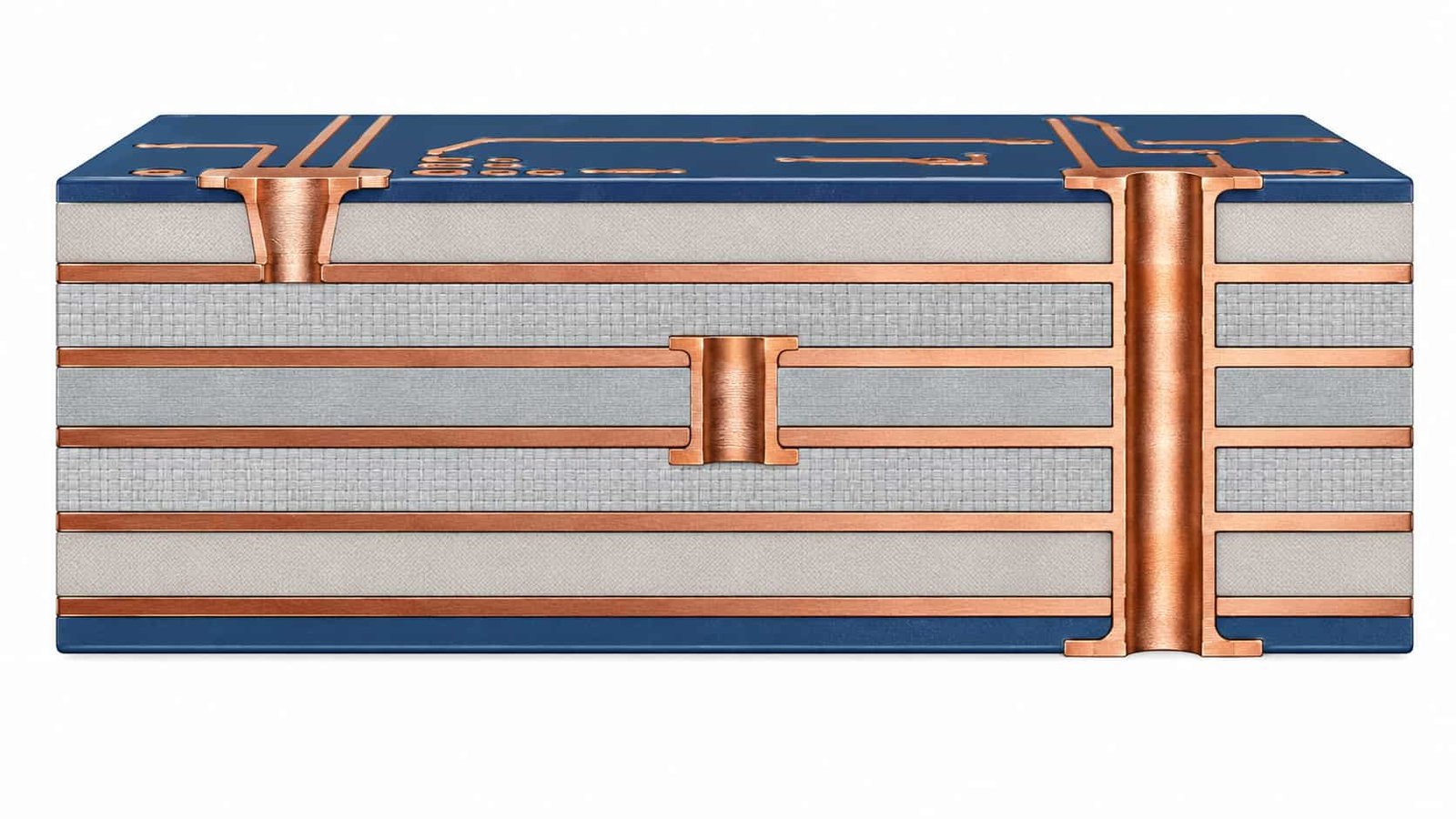
Quick Summary
Key point: Standard HDI capability supports 1–3 stages of blind via. Advanced capability reaches 1–6 stages. Laser blind via minimum diameter is 3–4 mil depending on stage. PTFE boards are limited to 2 lamination cycles. Via fill quality and pad ring size must be confirmed before production.
Blind and buried vias in high frequency PCB require more lamination cycles, tighter process control, and more detailed stackup planning than simple through-hole designs. Projects using Rogers, PTFE, Taconic, or F4B materials with blind or buried vias need early engineering review to confirm feasibility, layer registration, and signal integrity.
Types of Vias Used in High Frequency PCB
Before reviewing manufacturing limits, it helps to understand the three main via types used in multilayer high frequency PCB and why each is selected.
Through-Hole Via (PTH)
A through-hole via passes through all layers of the board from top to bottom. It is the simplest and lowest-cost via structure, but it occupies pad space on every layer and may create signal stubs in high frequency circuits. Back drilling can remove part of the stub, but this adds process steps.
For stub removal in high frequency boards, see Back Drill PCB: What It Is, When You Need It, and Manufacturing Limits.
Blind Via
A blind via connects an outer layer to one or more inner layers without passing through the entire board. It is visible from one surface but does not exit the opposite side. Blind vias reduce signal stubs, save inner layer space, and allow finer via pitch in compact RF designs.
Buried Via
A buried via connects two or more inner layers and is not visible from either outer surface. It requires an additional lamination cycle to form before the outer layers are added. Buried vias are used in designs where inner layer routing density is critical and outer layer pad space must be conserved.
Blind and Buried Via Specifications for High Frequency PCB
The table below summarizes standard and advanced manufacturing capabilities for blind via, buried via, and HDI structures in high frequency PCB.
Parameter | Standard Capability | Advanced Capability |
HDI stages supported | 1–3 stages | 1–6 stages |
Laser blind via diameter | 4–6 mil | 3–6 mil |
Laser blind via dielectric thickness | 0.065 mm (1080H) | 0.05 mm (106H) |
Laser blind via aspect ratio | 0.5:1 – 0.8:1 | ≤ 0.9:1 |
Micro blind via fill: max convex | ≤ 50 µm | ≤ 50 µm |
Micro blind via fill: max concave | ≤ 127 µm | ≤ 76 µm |
Bottom pad ring (1st stage) | D + 8 mil | D + 6 mil |
Bottom pad ring (2nd stage+) | D + 8 mil | D + 6 mil |
FR4 / High-speed FR4 lamination | ≤ 3 times | ≤ 3 times |
PTFE lamination | ≤ 2 times | ≤ 2 times |
Layer count range | 1–32 layers | 1–50 layers |
Note: Advanced capability specifications require engineering review. PTFE and Rogers PTFE-based materials have additional constraints on lamination count and via processing. Not all layer counts and stage combinations are automatically feasible — stackup review is required before order confirmation.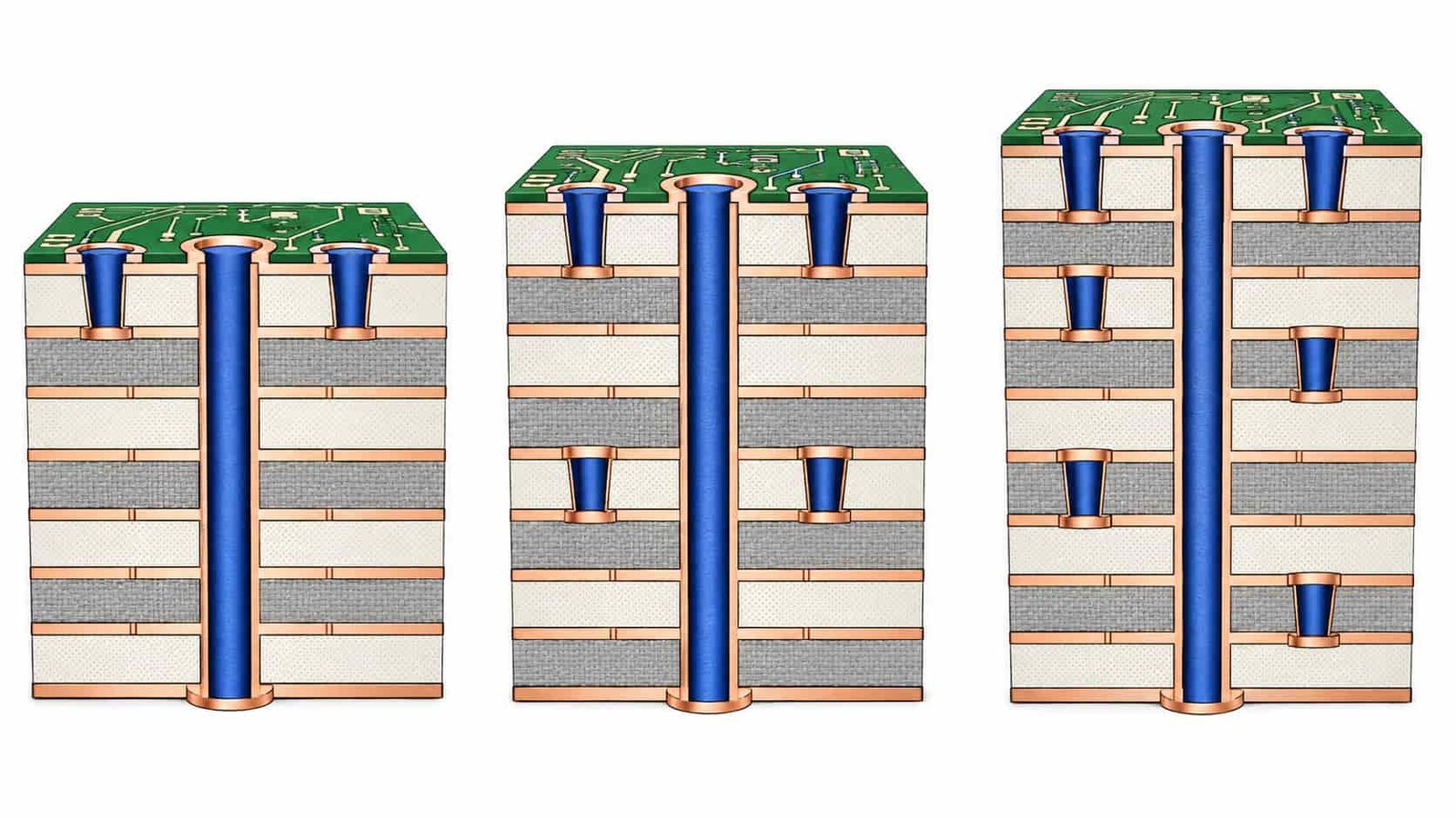
HDI Stage Limits for High Frequency PCB
HDI (High Density Interconnect) stage count refers to how many sequential lamination and laser drilling cycles are used to build up the blind via structure. Each stage adds one set of blind vias at a different depth level.
1-Stage HDI
The most common HDI structure for RF and microwave PCB. Laser blind vias connect the outer layer to the first inner layer only. One additional lamination cycle is required compared to a standard through-hole board. Suitable for most compact RF modules, antenna PCB, and 5G component boards.
2-Stage and 3-Stage HDI
2-stage and 3-stage HDI allows blind vias to reach deeper inner layers. Each stage requires an additional lamination cycle. This increases total build time, lamination count, registration requirements, and cost. Used in high-density microwave modules, radar signal processing boards, and multi-channel RF systems with complex routing requirements.
4-Stage to 6-Stage HDI
Advanced capability only. Requires engineering review for each project. Layer registration tolerance, material compatibility, warpage control, and lamination count limits must all be confirmed before production begins. Not all materials support this many lamination cycles.
Design tip: For most RF and microwave PCB projects, 1-stage HDI is sufficient and provides a good balance between via density, cost, and manufacturing reliability. Higher stage counts should only be used when required by the routing design and confirmed with the manufacturer.
Laser Blind Via Specifications
Laser blind vias in high frequency PCB are formed by CO2 or UV laser drilling. The via diameter, dielectric thickness, aspect ratio, and fill quality all affect RF signal behavior and long-term reliability.
Laser Via Diameter
- Standard capability: 4–6 mil laser blind via diameter
- Advanced capability: 3–6 mil laser blind via diameter
- Smaller via diameters require thinner dielectric and more precise laser control
- Via diameter also affects pad ring size and routing density
Dielectric Thickness for Laser Blind Via
- Standard: 0.065 mm using 1080 prepreg (H grade)
- Standard: 0.09 mm using two layers of 106 prepreg
- Advanced: 0.05 mm using 106 prepreg (H grade)
- Advanced: 0.06 mm using one layer of 1080 prepreg
Thinner dielectric allows smaller via diameter and finer HDI structures but requires tighter lamination control and material selection.
Laser Via Aspect Ratio
- Standard: 0.5:1 to 0.8:1
- Advanced: up to 0.9:1
Laser via aspect ratio is the ratio of dielectric thickness to via diameter. Keeping the aspect ratio within the recommended range supports reliable copper fill and plating inside the via.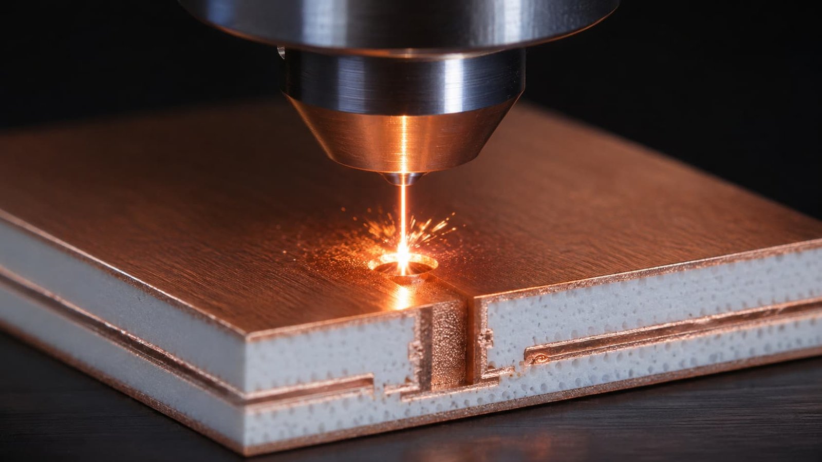
Micro Blind Via Fill Quality
For high frequency PCB, especially those using stacked or staggered blind vias in HDI designs, via fill quality affects surface planarity, pad reliability, and signal behavior at RF frequencies.
Fill Quality Specifications
- Maximum convex (bump above surface): ≤ 50 µm — both standard and advanced
- Maximum concave (dimple below surface): ≤ 127 µm standard, ≤ 76 µm advanced
- Fill quality is governed by IPC-6012C Table 3-10 capped plating requirements
Poor via fill can create surface irregularities that affect solder paste printing, component placement, and RF pad quality. For stacked blind vias — where a second laser via is drilled on top of a filled first-stage via — fill planarity is especially critical.
Key point: Stacked blind vias require the first-stage via to be filled and planarized before the second stage is drilled. Any concavity or surface roughness at the first stage can affect the accuracy of the second laser drilling step.
Blind Via Pad Ring Requirements
Pad ring size for blind vias must be confirmed in the stackup review. The pad ring provides the copper contact area around the via hole and affects drill registration tolerance and via reliability.
- 1st stage blind via: bottom pad ring = via diameter D + 8 mil (standard), D + 6 mil (advanced)
- 2nd stage and above: same pad ring rule applies to each stacked via
- Pad ring must account for layer registration tolerance and laser positioning accuracy
Pad ring requirements interact directly with trace and space design rules. For related context see How Copper Thickness Affects RF PCB Line Width and Manufacturing Tolerances.
Lamination Count Limits by Material
Each blind or buried via stage requires an additional lamination cycle. The maximum number of lamination cycles depends on the material type used in the stackup.
FR4 and High-Speed FR4
Maximum 3 lamination cycles. This supports up to 3-stage HDI blind via structures in standard FR4 and high-speed FR4 materials. Most multilayer RF PCB using FR4 or hybrid FR4 + Rogers constructions fall within this limit.
PTFE-Based Materials
Maximum 2 lamination cycles. PTFE materials are more sensitive to repeated thermal cycles than FR4. Exceeding the lamination limit may cause material degradation, delamination, or dimensional instability.
For more on PTFE processing constraints, see PTFE PCB Manufacturing Challenges and Process Considerations.
Hybrid Stackups (FR4 + Rogers or PTFE)
Hybrid stackups combining FR4 with Rogers or PTFE materials must follow the lower lamination limit of the two materials. If PTFE is included in any layer, the 2-cycle limit applies to the entire stackup. Material compatibility, bonding system, and layer sequence must be reviewed before production.
For hybrid stackup design background, see FR4 + Rogers Hybrid PCB Stackup: When Should You Use It?.
Blind Via in RF Signal Path: Design Considerations
When a blind via is used in an RF signal path — for example, at a layer transition in a microwave circuit or antenna feed network — its electrical behavior must be considered alongside its physical dimensions.
- Blind via inductance depends on via diameter, depth, and pad size
- At microwave frequencies, via inductance can cause impedance mismatch and insertion loss
- Back-to-back blind vias (stacked) should be reviewed for stub contribution
- Via fences around RF blind vias help maintain ground reference and reduce radiation
- Laser via diameter and depth should be included in field solver simulation for high-frequency critical paths
For overall via design guidance in RF circuits, see Via Design Considerations for RF PCB Manufacturing. For stackup planning context, see RF PCB Stackup Design: Key Factors Before Manufacturing.
Controlled Impedance and Blind Via Interaction
Many high frequency PCB with blind or buried vias also require controlled impedance. The two requirements interact in several ways that must be reviewed during stackup planning.
- Dielectric thickness for laser blind vias affects impedance of adjacent signal layers
- Copper balance across layers affects final board thickness and Dk uniformity
- Lamination pressure and temperature profile can shift dielectric thickness slightly
- Impedance targets should be calculated using the confirmed production stackup, not nominal datasheet values
For impedance control background, see Why Controlled Impedance Matters in RF PCB Manufacturing.
Information Needed for Blind and Buried Via PCB Quotation
To review feasibility and provide an accurate quotation, the following information should be included:
- Gerber files (all layers)
- NC drill files including blind and buried via definitions
- Complete PCB stackup with layer sequence, dielectric materials, and thickness
- Via structure: blind, buried, through-hole, stacked, or staggered
- HDI stage count requirement
- Material type — FR4, Rogers, PTFE, Taconic, F4B, or hybrid
- Layer count
- Controlled impedance requirements
- Surface finish
- Quantity — prototype or batch
- Working frequency or application background
For a full quotation checklist, see What Files Are Needed for a High Frequency PCB Quotation?.
Conclusion
Blind and buried vias in high frequency PCB allow more compact routing, reduced through-hole stubs, and better RF performance in multilayer designs. Standard capability supports 1–3 HDI stages with laser blind via diameter from 4–6 mil. Advanced capability extends to 1–6 stages with 3–6 mil laser via diameter.
PTFE and Rogers PTFE-based materials are limited to 2 lamination cycles. Stackup review, layer registration, via fill quality, pad ring size, lamination count, and controlled impedance must all be confirmed before production begins. Early engineering review reduces risk and supports consistent prototype and batch production results.