Vias are the source of many RF PCB signal integrity problems that are not immediately obvious at lower frequencies. At RF and microwave frequencies, via structures that are electrically transparent at 1 GHz become significant impedance discontinuities at 10 GHz, resonant stubs at 20 GHz, and sources of spurious radiation at Ka-band. Understanding the RF behavior of vias — and designing them correctly from the start — avoids costly board respins.
As a direct high frequency PCB factory producing Rogers, PTFE, and hybrid multilayer RF PCB, we review via structures in every DFM review. This guide covers the most important via design considerations for RF and microwave PCB.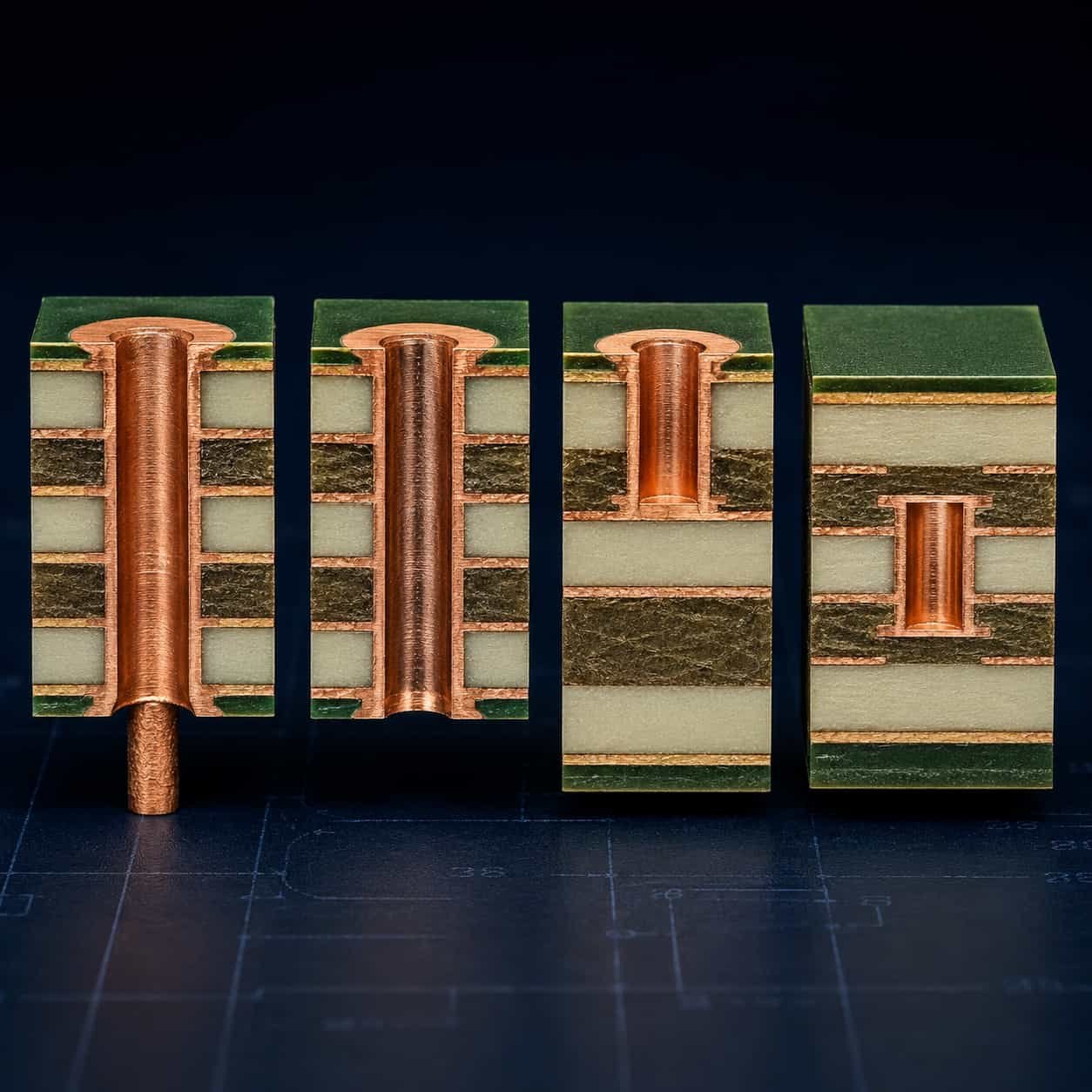
Quick Summary
Key point: The three most important via design considerations for RF PCB are: (1) via stub resonance — a through-hole via in a multilayer board creates a stub below the signal layer that resonates and causes insertion loss at a frequency determined by stub length; back drill removes the stub for designs above approximately 10 GHz; (2) via fence — rows of ground vias flanking a microstrip or stripline trace prevent signal coupling to adjacent circuits and reduce radiation; (3) aspect ratio — the ratio of board thickness to via diameter must stay within the factory’s confirmed limit (14:1 advanced, 10:1 standard) or the via plating will be unreliable.
Via Types in RF PCB
Through-Hole Via (PTH)
A through-hole via connects copper layers from the top surface to the bottom surface of the PCB, passing through all dielectric layers. It is the simplest and lowest-cost via type.
- Plated barrel: electroplated copper connecting all layers
- Signal via: carries RF signal from one layer to another
- Ground via: connects ground planes on different layers — essential for return current path
- Via fence: array of ground vias for signal isolation
- RF limitation: via stub (unused barrel below signal layer) creates resonance at high frequencies
Blind Via
A blind via starts at an outer layer and terminates at an inner layer — it does not go all the way through the board. Blind vias reduce via stub resonance by eliminating the stub below the signal layer.
- Layer 1 to layer 2 blind via: connects top layer to first inner layer only
- Advantage: no via stub below the signal layer — better RF performance at high frequencies
- Manufacturing cost: higher than through-hole — requires an additional lamination press cycle
- PTFE materials: maximum 2 press cycles — limits blind via stages in PTFE designs
For blind via manufacturing details, see Blind and Buried Via Capabilities in High Frequency PCB
Back-Drilled Via
Back drilling mechanically removes the unused via stub from the back side of a through-hole via, reducing stub length to a specified target (typically ≤10 mil stub remaining).
- Process: after board completion, a slightly larger drill bit enters from the back and removes the stub barrel
- Target stub length: ≤10 mil (0.25mm) — specify in design documentation
- Depth tolerance: ±0.1mm — confirm with factory
- Advantage: achieves near-blind-via RF performance at lower cost than genuine blind via
- Limitation: stub is not eliminated, only shortened — for highest frequencies, blind via is better
For back drill specification, see Back Drill PCB: Via Stub Elimination for High Frequency Designs
Via Stub Resonance: The Most Important RF Via Problem
When an RF signal travels from the top layer of a multilayer PCB to an inner layer through a through-hole via, only the portion of the via from the top to the target layer carries the signal. The remaining via barrel below the target layer acts as an open-ended stub — a transmission line stub connected in shunt with the signal path.
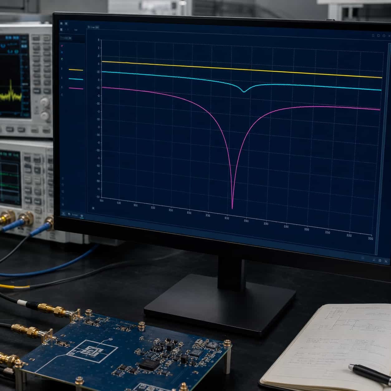
This stub resonates at a frequency determined by its length. At resonance, the stub presents a low impedance to ground, pulling signal energy off the main transmission line and creating a notch in the insertion loss response.
Stub Resonance Frequency
- Quarter-wave resonance: stub resonates when its electrical length is a quarter wavelength
- Resonance frequency formula: f = c / (4 × stub_length × √Dk)
- Example: 2mm stub in Rogers RO4350B (Dk 3.48): f = 3×10⁸ / (4 × 0.002 × √3.48) ≈ 20 GHz
- Example: 1mm stub: resonance at approximately 40 GHz
- At resonance: 3–15 dB insertion loss depending on stub diameter and proximity to signal layer
- Impact: creates a frequency notch in the transmission response — may fall in or near the operating band
When Via Stub Resonance Matters
- Below 5 GHz: via stub resonance typically above 30 GHz for standard board thicknesses — no concern
- 5–15 GHz: stub resonance may be in or near band for thick boards or long stubs — evaluate
- Above 15 GHz: stub resonance is almost always a concern — back drill or blind via required
- Ka-band (26.5–40 GHz): even short stubs (0.5mm) resonate in band — blind via mandatory
Solutions: Back Drill or Blind Via
- Back drill: reduces stub length to ≤10 mil — moves resonance well above operating frequency for most X-band designs
- Blind via: eliminates stub entirely — best solution for Ka-band and above
- Via-in-pad with copper fill: for QFN and flip-chip designs where via is directly under pad — eliminates stub and improves thermal
Anti-Pad Design for Impedance Continuity
The anti-pad is the clearance hole in a ground plane layer where a signal via passes through. The size of the anti-pad affects the impedance of the via transition — too small an anti-pad increases parasitic capacitance and shifts the via impedance down from the target.
- Standard anti-pad: via pad + 0.2–0.5mm clearance — adequate for most RF designs below 10 GHz
- Optimized anti-pad: sized to match via impedance to 50Ω — important above 10 GHz
- Rule of thumb: anti-pad diameter ≈ 3× via drill diameter for good impedance continuity at X-band
- For Ka-band: anti-pad optimization is critical — typically requires EM simulation to confirm via impedance
- Back-drill anti-pad: the back-drill diameter must be slightly larger than the original via — confirm with factory
Factory DFM: We flag anti-pad sizes that are likely to cause impedance discontinuity at the specified operating frequency during DFM review. For Ka-band designs, we recommend the designer run EM simulation of the via transition before finalizing the layout.
Via Fence Design for RF Signal Isolation
A via fence (also called a picket fence or via wall) is a row or double row of ground vias placed parallel to a microstrip or stripline trace. The via fence prevents the transmission line from coupling energy to adjacent circuits and reduces radiation from the trace.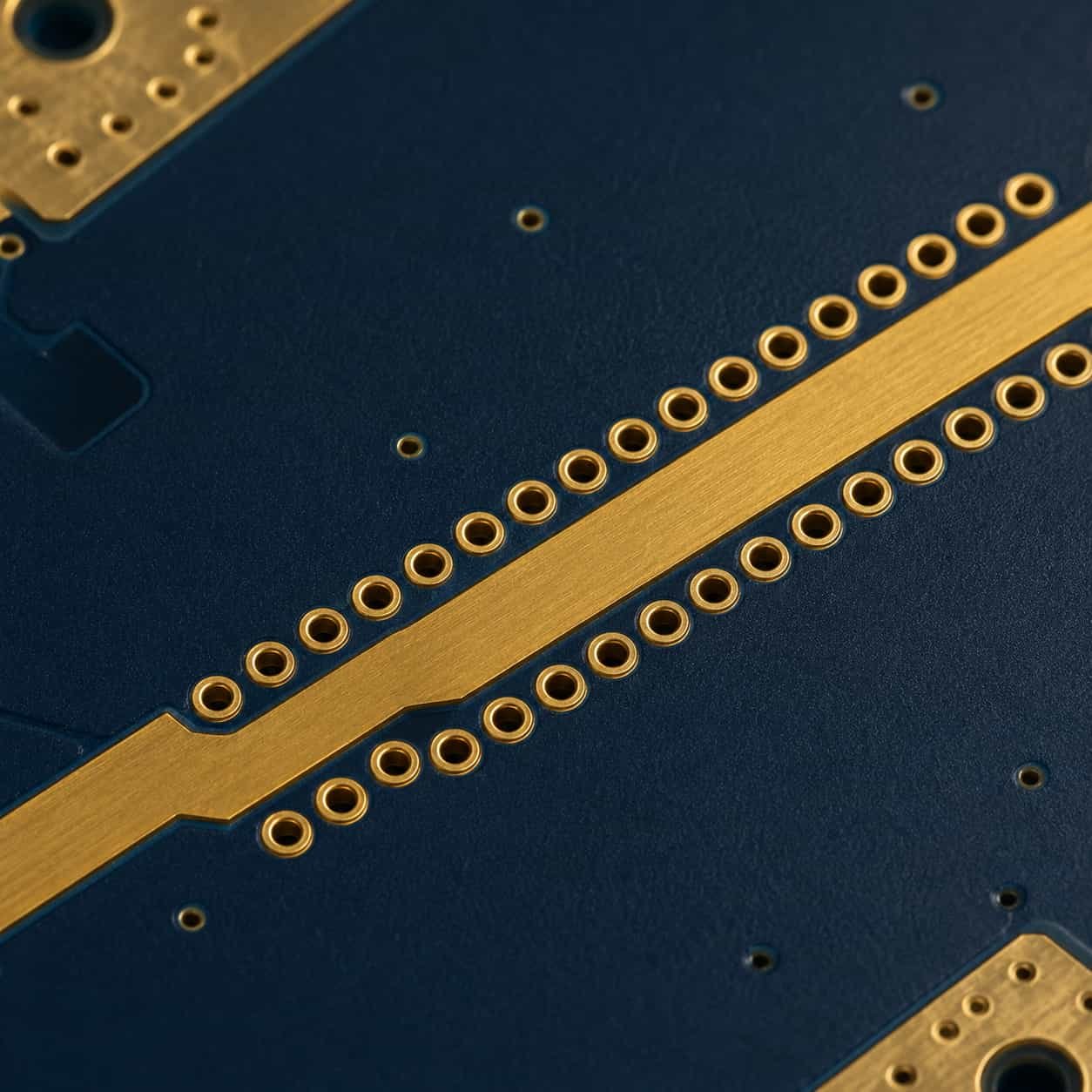
Via Fence Design Rules
- Via spacing along the fence: maximum λ/10 at the highest operating frequency — prevents signal leakage between vias
- At 10 GHz in RO4350B (Dk 3.48): λ/10 = 3×10⁸ / (10×10⁹ × √3.48) / 10 ≈ 1.6mm — max via pitch
- At 24 GHz: max via pitch ≈ 0.67mm — tight pitch required
- Via diameter: typically 0.2–0.3mm for fence vias — smaller diameter allows tighter pitch
- Distance from trace: fence via should be within 1–2 trace widths from the edge of the microstrip trace
- Both sides: via fence on both sides of the trace for maximum isolation
- Through the full stackup: fence vias should connect top ground to bottom ground through all layers
When Via Fence Is Required
- High isolation circuits: LNA input / PA output separation — fence prevents reverse coupling
- Phased array antenna feed networks: prevents inter-element coupling through the substrate
- Circuits with tight adjacent channel spacing
- Above 10 GHz: via fence is standard practice for isolation-critical circuits
- Board edge: via fence along board edge prevents radiation from edge currents
Aspect Ratio: Via Diameter vs Board Thickness
Aspect ratio is the ratio of board thickness to via drill diameter. As aspect ratio increases, the via becomes more difficult to plate uniformly — the electroplating solution has difficulty reaching the center of a deep, narrow hole. Vias with excessive aspect ratio have thin plating at the center of the barrel, leading to early failure under thermal cycling.
Aspect Ratio Limits
- Standard: 10:1 — a 0.2mm via in a 2.0mm board
- Advanced: 14:1 — a 0.2mm via in a 2.8mm board
- Extreme limit: 15:1 — requires special evaluation
- PTFE materials: same aspect ratio limits as FR4 — 10:1 standard, 14:1 advanced
Practical Via Sizing for RF PCB
- Signal via at X-band: 0.2–0.3mm drill, 0.4–0.5mm pad — compact, low parasitic
- Ground via (fence): 0.2mm drill, 0.35–0.4mm pad — allows tight pitch
- Power via: 0.3–0.5mm drill — larger for current carrying capacity
- Thermal via under component: 0.15–0.25mm drill, tightly spaced array
- For thick boards (>2.0mm): confirm via diameter against aspect ratio limit with factory before finalizing
Annular Ring Requirements
The annular ring is the copper ring around the via hole on each copper layer. It must be large enough to ensure electrical continuity even with the worst-case drill registration tolerance.
- IPC Class 2 outer layer: minimum 0.05mm annular ring after worst-case drill offset
- IPC Class 2 inner layer: breakout (touching the hole edge) permitted
- IPC Class 3 outer layer: minimum 0.05mm — same as Class 2
- IPC Class 3 inner layer: NO breakout permitted — minimum annular ring on every inner layer
- Practical design rule: target 0.1–0.15mm annular ring for robust manufacturing yield
- Pad size: via drill diameter + 2 × (annular ring + drill tolerance) = pad diameter
IPC Class 3 impact: Specifying IPC Class 3 requires confirmed annular ring on every inner layer — no breakout permitted. This drives a larger minimum pad size than Class 2. For dense multilayer designs at Class 3, confirm minimum pad size with the factory during DFM review before routing.
Blind Via Planning for PTFE Materials
For multilayer PCB using Rogers RO3003, RT5880, or other PTFE materials, the 2-cycle lamination limit constrains the number of blind via stages that can be built.
- Through-hole only: 1 lamination cycle (for the base stackup) — leaves 1 remaining cycle for 1 blind via stage
- 1 blind via stage (e.g. layer 1–2): 2 cycles total — at the PTFE limit
- 2 blind via stages: 3 cycles — NOT possible with PTFE materials
- Rogers RO4350B and RO4003C: 3 cycles maximum — allows 2 blind via stages
- Design rule: plan blind via stages before selecting PTFE material — confirm total cycle count
For PTFE lamination cycle limits, see PTFE PCB: Material Properties, Manufacturing Process and Applications. For stackup design, see RF PCB Stackup Design: Key Factors Before Manufacturing.
IPC Class 3 Via Copper Plating
Via copper plating quality is more critical in RF PCB than in digital PCB because via barrel resistance affects insertion loss, and via fatigue under thermal cycling is a reliability concern over the product’s service life.
- IPC Class 2: 20 µm average PTH copper plating — minimum for RF PCB
- IPC Class 3: 25 µm average with 20 µm minimum at any point — recommended for aerospace, defense, and industrial RF PCB
- Verification: microsection FAI — cross-section photo showing copper plating thickness at barrel center
- Void limit: Class 3 maximum 5% void per hole, Class 2 maximum 10%
- Thermal cycling reliability: thicker plating (25 µm vs 20 µm) provides significantly better via fatigue life
- PTFE materials: via plating quality is critical — without plasma activation the copper bonds weakly regardless of thickness
Via Design Summary: Practical Rules for RF PCB
What to Include in Your Via Specification
- Via drill diameter and pad diameter for each via type
- Blind via stages if applicable — with start and stop layer
- Back drill requirement — target stub length and depth tolerance
- Via fence pitch — specify maximum pitch at operating frequency
- IPC Class for via copper plating — Class 2 or Class 3
- Via fill requirement — copper fill, resin fill, or open
- Aspect ratio confirmation — for thick boards or small vias, confirm against factory limit
For quotation file checklist, see What Files Are Needed for a High Frequency PCB Quotation?. For drilling capability, see Drilling Capabilities for High Frequency PCB.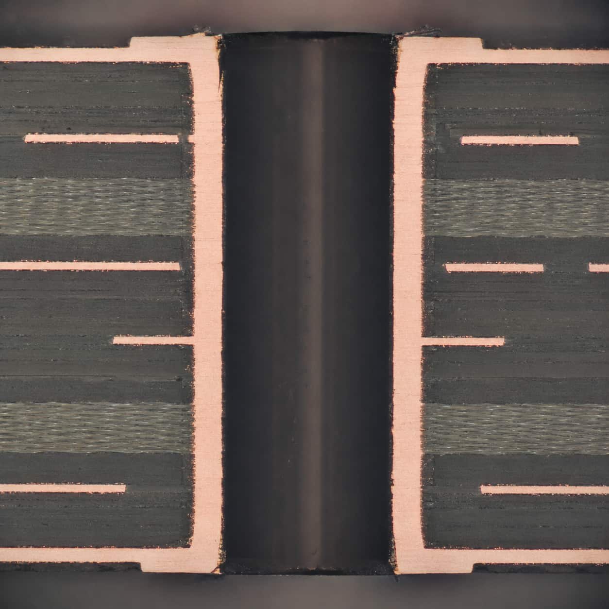
Conclusion
Via design for RF PCB requires attention to three problems that do not exist at lower frequencies: via stub resonance (solved by back drilling or blind via), ground via fence design for signal isolation, and aspect ratio compliance for reliable plating. For PTFE materials, the 2-cycle lamination limit adds an important constraint on blind via structure complexity that must be planned before selecting the material.
As a direct high frequency PCB factory, we review via structures — stub resonance risk, aspect ratio, annular ring, and lamination cycle count — in every DFM review before production. Via problems caught in DFM cost nothing to fix. The same problem found after production costs the full board price and the lead time.