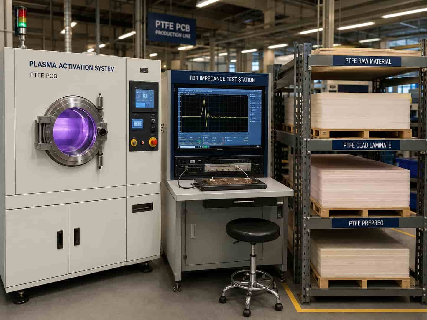
PTFE — polytetrafluoroethylene — is a synthetic fluoropolymer that provides the lowest dielectric loss of any commercially available PCB laminate material. At frequencies above 20 GHz, and in wide-band systems covering 2–18 GHz or more, PTFE is the material that RF and microwave engineers reach for when Rogers RO4350B or RO4003C can no longer meet the insertion loss budget.
PTFE PCB is not a single material — it is a family of laminates that all use PTFE as their base polymer. Rogers RT5880, Rogers RO3003, Taconic TLY-5, Taconic RF-35, and F4BM220 are all PTFE-based. What they share is the same fundamental advantage — very low Df — and the same fundamental manufacturing challenge: PTFE does not bond to copper without specialized surface preparation. This guide explains what PTFE PCB is, how it differs from FR4 and Rogers hydrocarbon materials, and what manufacturing processes a factory must have to produce reliable PTFE PCB.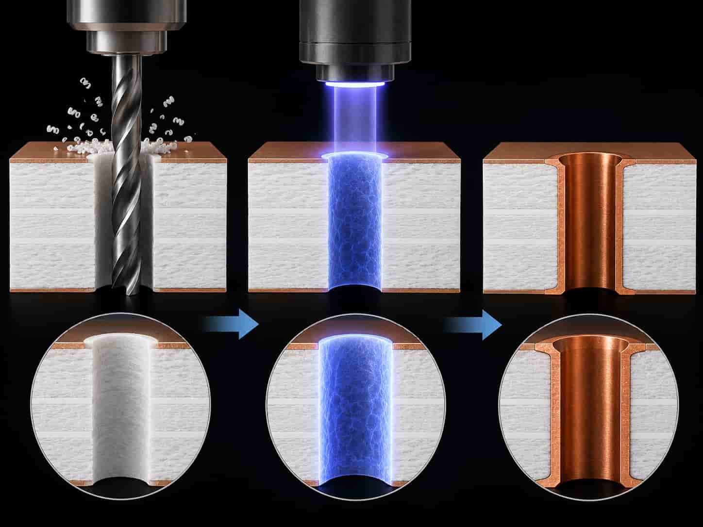
Quick Summary
Key point: PTFE PCB uses polytetrafluoroethylene as the laminate base material, providing Df as low as 0.0009 — 4× lower than Rogers RO4350B and 20× lower than standard FR4. PTFE is required for Ka-band and above, wideband EW systems covering 2–18 GHz, W-band applications, and aerospace designs where maximum insertion loss stability over a wide temperature range is mandatory. PTFE requires hole wall activation before copper plating — either plasma etch or sodium naphthalene treatment — without which PTH reliability will fail under thermal cycling.
What Is PTFE and Why Is It Used in High Frequency PCB?
Polytetrafluoroethylene (PTFE) is a fluoropolymer first synthesized in 1938 and commercially produced from the 1940s. Its molecular structure — a carbon backbone fully shielded by fluorine atoms — gives it exceptional chemical inertness and, critically for PCB applications, extremely low dielectric loss across a wide frequency range.
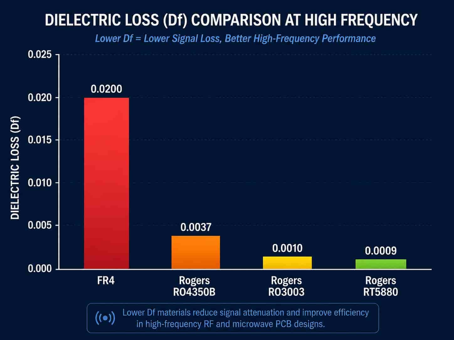
In a PCB dielectric, every watt of RF signal power passing through the material loses some fraction as heat. This loss is proportional to the dissipation factor (Df). FR4 has Df of approximately 0.020 at high frequencies. Rogers RO4350B has Df of 0.0037. Rogers RT5880 — a PTFE glass composite — has Df of 0.0009. At 10 GHz over a 6-inch feed line, the difference between FR4 and RT5880 can amount to several dB of additional insertion loss. For a receiver system, every dB of insertion loss before the LNA adds directly to the noise figure.
- FR4 Df at 10 GHz: approximately 0.020 — acceptable below 1 GHz for short traces
- Rogers RO4350B Df at 10 GHz: 0.0037 — standard for most RF and microwave designs to X-band
- Rogers RO3003 Df at 10 GHz: 0.0010 — PTFE ceramic, Ka-band and defense applications
- Rogers RT5880 Df at 10 GHz: 0.0009 — PTFE glass, lowest-loss standard PCB material
- Taconic TLP-5 Df at 10 GHz: 0.0009 — PTFE glass, equal to RT5880
PTFE PCB vs Rogers RO4350B: The Key Distinction
A common source of confusion: Rogers RO4350B is often called a ‘Rogers PCB’ but it is NOT a PTFE material. RO4350B is a hydrocarbon ceramic laminate — it processes on standard FR4 equipment without PTFE-specific activation. Only the Rogers RO3000 series and RT/duroid series are true PTFE materials.
Important clarification: When engineers say ‘PTFE PCB’ they typically mean boards using Rogers RO3003, RT5880, Taconic TLY-5, or F4B PTFE materials — not Rogers RO4350B. RO4350B is a hydrocarbon material that does not require PTFE-specific manufacturing processes. This distinction is critical when specifying a PCB to a manufacturer — a factory that handles RO4350B but not RO3003 does not have true PTFE capability.
Which Rogers and Taconic Grades Are PTFE Materials?
The following materials are PTFE-based and require the full PTFE manufacturing process including hole wall activation:
Rogers PTFE Materials
- Rogers RO3003 (Dk 3.0, Df 0.0010) — PTFE ceramic, Ka-band radar, 77GHz automotive, aerospace AESA
- Rogers RO3003G2 (Dk 3.0, Df 0.0010) — tighter Dk tolerance ±0.03, automotive radar production
- Rogers RO3006 (Dk 6.15, Df 0.0020) — high Dk PTFE, compact antenna design
- Rogers RO3010 (Dk 10.2, Df 0.0022) — maximum Dk PTFE, filter miniaturization
- Rogers RT5880 (Dk 2.2, Df 0.0009) — PTFE glass, EW, SIGINT, W-band, ultra-low loss
- Rogers RT5870 (Dk 2.33, Df 0.0012) — PTFE glass, slightly higher Dk than RT5880
Taconic PTFE Materials
- Taconic TLY-5A / TLP-5 / TLY-5 (Dk 2.17–2.22, Df 0.0009) — equal to Rogers RT5880 in performance
- Taconic TLY-3 (Dk 2.33, Df 0.0012) — equal to Rogers RT5870
- Taconic RF-35 (Dk 3.5, Df 0.0018) — lower Df than Rogers RO4350B at similar Dk
- Taconic RF-60A (Dk 6.5, Df 0.0038) — high Dk PTFE
- Taconic CER-10 (Dk 10.0, Df 0.0035) — very high Dk PTFE ceramic
F4B PTFE Materials
- F4BM220 (Dk 2.20, Df 0.0010) — cost-effective PTFE, commercial applications below 20 GHz
- F4BM255 (Dk 2.55, Df 0.0013) — mid-range PTFE for commercial RF
- F4BTM400 through F4BTM615 — higher Dk F4B PTFE grades
For Rogers material selection details, see Rogers PCB Material Selection Guide. For Taconic material comparison, see Taconic PCB Materials for RF and Microwave Applications.
PTFE PCB Manufacturing: What Makes It Different
PTFE is chemically inert — this is the same property that makes it low-loss for RF signals, but it also means that copper does not naturally adhere to PTFE surfaces during the electroless copper plating step that creates through-hole connections. Without special preparation of the drilled hole wall, the copper plating will not bond reliably to the PTFE. The PTH will pass initial electrical testing and fail weeks later when the assembly is thermally cycled.
This is the reason that PTFE PCB manufacturing is a specialized process that not every PCB factory can reliably perform. The factory must have one of two hole wall activation methods:
Method 1: Plasma Activation
A plasma chamber generates an RF plasma (typically using oxygen or argon/oxygen mixture) that etches the PTFE hole wall surface at the molecular level, creating polar functional groups that accept electroless copper deposition. Plasma activation is the cleaner process — no hazardous chemical waste, consistent activation depth, and compatible with tight-tolerance drilling.
- Equipment: dedicated plasma activation chamber
- Process: 5–15 minutes exposure depending on board thickness and hole diameter
- Result: hole wall surface becomes receptive to electroless copper
- Our factory: plasma activation is our standard PTFE process
Method 2: Sodium Naphthalene (Wet Chemical) Activation
A sodium naphthalene solution in tetrahydrofuran etches the PTFE surface chemically, removing fluorine atoms and creating a bondable surface. This method works well but requires careful chemical handling and waste disposal. It is less common in modern factories due to environmental and safety considerations.
- Equipment: wet chemical treatment line
- Effective for all PTFE grades
- Requires chemical hazard management
PTFE-Specific Drilling
PTFE is mechanically softer than FR4 and Rogers hydrocarbon materials. Standard FR4 drill parameters — spindle speed, feed rate, chip load — cause hole wall deformation, burring, and resin smear in PTFE boards. PTFE-specific drill parameters include:
- Lower spindle speed: prevents PTFE from melting at the drill tip from frictional heat
- Lower feed rate: reduces mechanical stress and prevents hole wall deformation
- PTFE-specific entry and backing materials: prevents surface burring at drill entry and exit
- More frequent drill bit replacement: PTFE work hardens drill edges faster than FR4
Lamination
- PTFE-specific press temperature profile: PTFE softens at different temperatures than FR4
- Controlled press pressure: PTFE will flow under excessive pressure — dimensional control requires careful press management
- Bonding film: Rogers 2929 bondply or Taconic tacBOND for PTFE-to-PTFE or PTFE-to-FR4 bonds — standard FR4 prepreg is not compatible
- Maximum 2 lamination press cycles: PTFE properties degrade with repeated thermal cycling above this limit
Controlled Impedance on PTFE
Impedance control for PTFE PCB requires using the confirmed production Dk value from the material certificate — not the nominal datasheet value. Taconic TLP-5 nominal Dk is 2.2 ±0.02; the actual production value may be 2.19 or 2.21. This 0.5% Dk difference produces a measurable impedance shift on Ka-band traces.
- Standard impedance tolerance: ±10% for traces ≥50Ω
- Advanced tolerance: ±8%
- Verification: TDR measurement on impedance coupons on every production panel
- Calculation: using confirmed production Dk from material certificate lot
For controlled impedance specification details, see Why Controlled Impedance Matters in RF PCB Manufacturing.
Applications That Require PTFE PCB
PTFE PCB is specified for applications where the lower Df of Rogers RO4350B or RO4003C is not sufficient. The key scenarios are:
Electronic Warfare Systems
Shipborne ESM, airborne RWR, and ground-based SIGINT systems covering 2–18 GHz or wider require consistent low Df across the entire band. Rogers RT5880 or Taconic TLY-5 are the standard choices — their Dk varies less than 2% from 1 GHz to 40 GHz, providing uniform insertion loss across the full EW band.
Ka-Band Radar and SATCOM
At Ka-band (26.5–40 GHz), Rogers RO3003 is the standard PTFE material. Antenna element dimensions at 35 GHz are approximately 3.5–4.0 mm — a 1% Dk variation shifts the resonant frequency by 350 MHz. RO3003’s tight Dk tolerance (±0.04) and very low Dk temperature coefficient (+13 ppm/°C) make it the preferred choice for Ka-band phased arrays, missile seekers, and satellite terminals.
W-Band (75–110 GHz)
Rogers RT5880 is the only standard PCB material suitable for W-band. At 77 GHz, antenna element dimensions are approximately 1.1 mm on RT5880 0.254 mm substrate. The minimum line width at this frequency is 2.5 mil — at the limit of standard advanced-process manufacturing capability.
Aerospace and Defense IPC Class 3
Defense programs requiring IPC Class 3, Rogers-certified material documentation, and 25-30 year record retention specify Rogers PTFE materials (RO3003, RT5880) for Ka-band and EW applications. Taconic PTFE materials require written customer approval to substitute for Rogers in defense programs.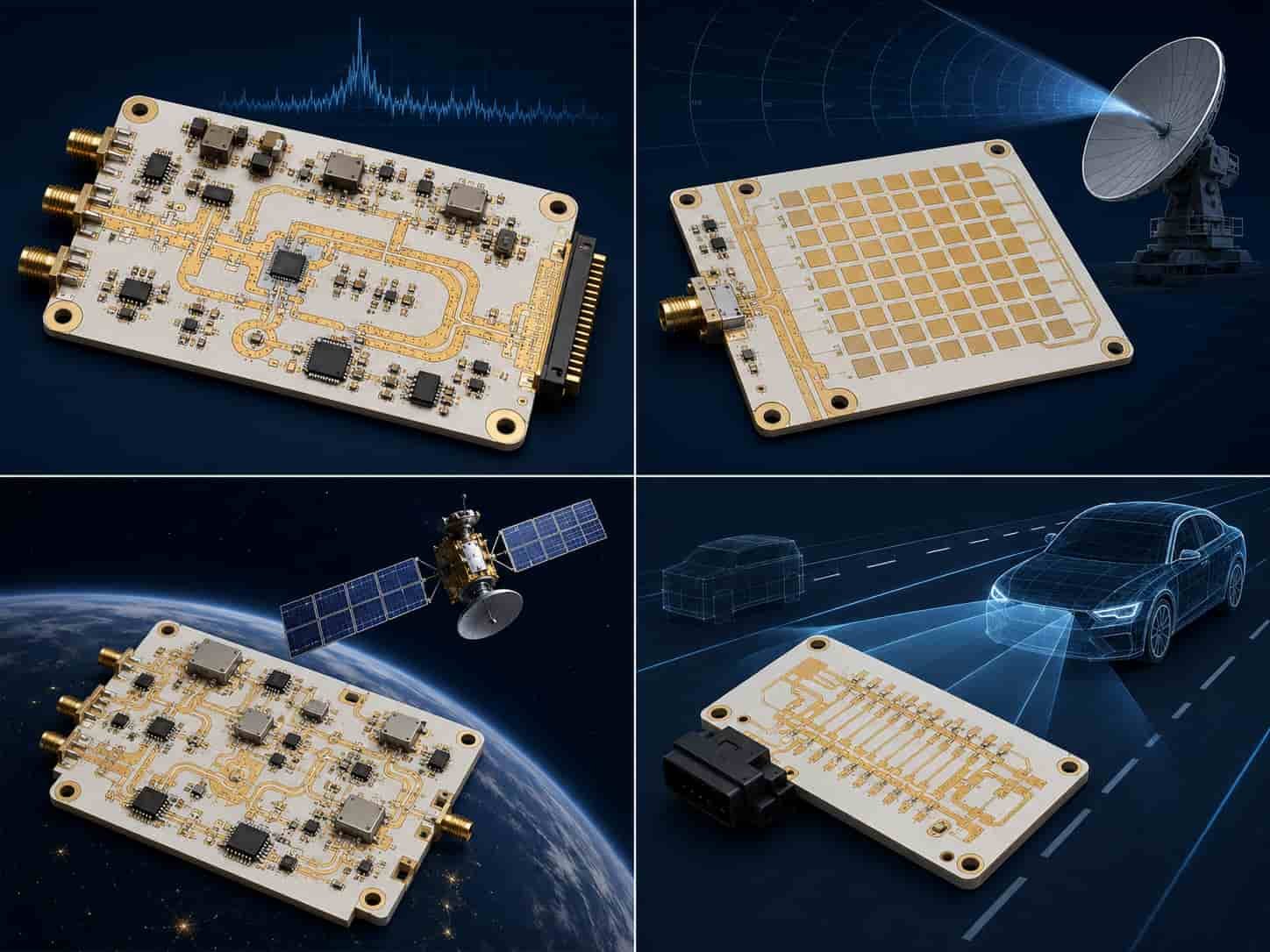
PTFE PCB Manufacturing Capability at Riching PCB
As a direct high frequency PCB factory, we process PTFE materials in regular production — not as an occasional special process. Our PTFE manufacturing capability:
- Hole wall activation: plasma activation process for all PTFE materials
- PTFE-specific drill parameters: confirmed parameters for Rogers RT5880, RO3003, Taconic TLY-5, RF-35, CER-10, F4B series
- Lamination: PTFE-specific press profiles, Rogers 2929 bondply for hybrid stackups
- Maximum lamination cycles: 2 cycles — strictly observed for all PTFE materials
- Controlled impedance: ±10% standard, ±8% advanced, TDR verified every lot
- Minimum drill diameter: 0.1 mm advanced, 0.2 mm standard
- Maximum aspect ratio: 14:1 advanced, 10:1 standard
- IPC Class 3: 25 µm average PTH copper plating, microsection FAI, 100% electrical test
- Materials in inventory: Rogers RT5880, RT5870, RO3003, RO3003G2, RO3006, RO3010; Taconic TLY-5A, TLP-5, TLY-5, TLY-3, RF-35, RF-60A, CER-10; F4BM220, F4BM255, F4BTM series
Factory note: The reliable test for whether a factory genuinely processes PTFE is to ask: ‘What hole wall activation method do you use for PTFE — plasma or sodium naphthalene?’ A factory that does not immediately answer this question does not regularly process PTFE. Proceeding without activation produces boards that pass initial test and fail under thermal cycling — a production quality problem that is expensive to discover after delivery.
How to Specify PTFE PCB for Your Design
When specifying PTFE PCB, the following information is needed for engineering review before production:
- PTFE material grade and manufacturer — Rogers RT5880, RO3003, Taconic TLP-5, F4BM220, etc.
- Substrate thickness — confirm standard availability for the specified grade
- Layer count and complete stackup with copper weight per layer
- Controlled impedance requirements — target value, tolerance, and layer
- Operating frequency or frequency range
- Application type — commercial or aerospace/defense with IPC Class 3
- Bonding film preference for hybrid stackups (Rogers 2929 or equivalent)
- Via structure — through-hole, blind, copper-filled
- Surface finish — ENIG or ENEPIG for aerospace, immersion silver for Ka-band and above
- Quantity — prototype, low-rate, or production
For a complete quotation file checklist, see What Files Are Needed for a High Frequency PCB Quotation?. For manufacturing challenges specific to PTFE, see PTFE PCB Manufacturing Challenges and Process Considerations.