Phased Array PCB: Material Selection, Design Rules and Manufacturing Guide
Substrate requirements, feed network design, Dk uniformity and manufacturing specifications for phased array antenna PCB — radar, satellite terminal and 5G mmWave applications.
Home » 5G mmWave PCB » Phased Array PCB: Material Selection, Design Rules and Manufacturing Guide
Table of Contents
Key point: Key point: Most factories quote 3–4 weeks waiting for RO3003 / RT5880 material procurement. Riching PCB maintains these materials in stock — no material wait.
Rogers RO3003 is a PTFE ceramic substrate with Dk 3.0 and Df 0.0010 — standard for Ka-band (26.5–40 GHz), 77 GHz automotive radar and 5G mmWave 28 GHz phased arrays. At 30 GHz, RO3003 insertion loss is ~0.5 dB/cm vs ~1.8 dB/cm for RO4350B. 50Ω microstrip on 0.127 mm RO3003 with 0.5 oz copper: ~0.28 mm trace width. Available thicknesses: 0.127 / 0.254 / 0.508 / 0.762 / 1.524 mm. All RO3003 orders require in-house plasma hole wall activation and maximum 2 lamination press cycles. Riching PCB stocks RO3003 in 0.127 mm and 0.254 mm with in-house plasma activation. No MOQ. Prototype 7–10 working days.Phased array PCB requires PTFE substrate with Dk uniformity of ±0.05 across the panel — not just nominal Dk. Rogers RO3003 (Dk 3.0, Df 0.0010) is standard for Ka-band and 5G mmWave arrays; RT5880 (Dk 2.20, Df 0.0009) for wideband and lowest-loss designs; RO4350B for S-band and C-band passive arrays. Impedance tolerance ±5% must be TDR-verified at multiple panel locations. All PTFE materials require in-house plasma activation. Riching PCB stocks RO3003, RT5880 and RO4350B with in-house plasma activation, panel-level TDR available. No MOQ. Prototype 5–10 working days.
Phased array PCB is one of the most demanding PCB manufacturing challenges because it combines the requirements of a high-frequency RF substrate with the need for consistent electrical performance across a large panel area. A single patch antenna element is forgiving — a small Dk variation shifts its resonance but the system still functions. An array of 64, 256, or 1024 elements is not forgiving: Dk variation across the panel creates phase errors between elements, degrading the beam pattern, reducing gain, and raising sidelobe levels.
This guide covers the PCB material requirements specific to phased array design, feed network architecture, stackup options, and manufacturing specifications.
Why Phased Array PCB Has Unique Requirements
Standard RF PCB design requires consistent impedance along a single transmission line. Phased array PCB requires consistent impedance and phase across hundreds or thousands of parallel transmission lines distributed across the entire panel. Any systematic or random variation in Dk across the substrate translates directly into phase errors at the antenna elements:
- At 28 GHz, a Dk variation of ±0.05 shifts patch antenna resonance by approximately 300–400 MHz
- A phase error of 5° between adjacent elements degrades array gain by approximately 0.4 dB and raises sidelobe levels
- For a 256-element array, even small systematic Dk gradients across the panel accumulate into beam pointing errors
This is why material Dk uniformity across the panel — not just nominal Dk value — is the critical specification for phased array PCB substrate.
Material Selection for Phased Array PCB
| Material | Dk | Df | Type | Phased Array Suitability |
|---|---|---|---|---|
| RO3003 | 3.0 | 0.0010 | PTFE ceramic | ✅ Best for most arrays — tight Dk tolerance, good thermal conductivity |
| RT5880 | 2.20 | 0.0009 | PTFE glass | ✅ Lowest loss — larger element size, lower thermal conductivity |
| RO4350B | 3.48 | 0.0037 | Hydrocarbon | ✅ S/C-band arrays — FR4-compatible, no plasma activation |
| Taconic TLY-5 | 2.17 | 0.0009 | PTFE glass | ✅ Suitable — similar to RT5880 |
| F4BM220 | 2.20 | 0.0010 | PTFE | ✅ Cost-effective — confirm Dk uniformity across panel |
| Standard FR4 | ~4.5 | ~0.020 | Epoxy glass | ⚠️ L-band only — not suitable above 2 GHz for arrays |
Rogers RO3003 — Standard for Ka-Band and 5G mmWave Arrays
RO3003 (Dk 3.0, Df 0.0010) is the most widely used substrate for Ka-band and 5G mmWave phased arrays. Its combination of tight Dk tolerance (±0.04 at 10 GHz), stable Dk over temperature (±0.05 from –40°C to +85°C), and higher thermal conductivity (0.50 W/m/K) compared to RT5880 makes it the preferred choice for high-power arrays where thermal management is a concern.
Rogers RT5880 — For Wideband and Lowest-Loss Arrays
RT5880 (Dk 2.20, Df 0.0009) offers the lowest insertion loss and is used where maximum array gain or wideband coverage is required. Lower Dk means larger antenna elements — for a fixed frequency, RT5880 elements are approximately 17% larger than RO3003 elements. Both RO3003 and RT5880 are available in multiple thicknesses from Riching PCB.
Rogers RO4350B — For S-Band and C-Band Arrays
For phased arrays operating below 8 GHz (S-band radar, C-band SATCOM), RO4350B (Df 0.0037) is acceptable — its higher Df is less significant at lower frequencies where absolute insertion loss per unit length is lower. RO4350B processes on FR4-compatible equipment with no plasma activation required. See RO4350B PCB guide for material properties.
Phased Array PCB Design Rules
| Parameter | Typical Value | Notes |
|---|---|---|
| Element spacing | λ/2 at center frequency | ~5 mm at 28 GHz on RO3003, ~13 mm at 10 GHz |
| Substrate thickness | 0.127–0.254 mm (Ka-band) | Thinner = narrower trace for 50Ω |
| Impedance tolerance | ±5% across panel | TDR at multiple panel locations — not edge only |
| Dk uniformity | ±0.05 across panel | Critical for phase uniformity between elements |
| Copper foil | Low-profile (Ka/Ku-band) | Reduces insertion loss in feed network |
| Surface finish | ENIG | Flat surface critical for element dimensional accuracy |
| PTFE lamination | Max 2 press cycles | All PTFE materials — exceeding causes Dk shift |
| Via drill (Ka-band) | 0.1–0.15 mm laser | Through-hole via transition loss significant at 28 GHz |
| Min. line width | 2.5 mil | Verify with fabricator for PTFE process |
Feed Network Architecture
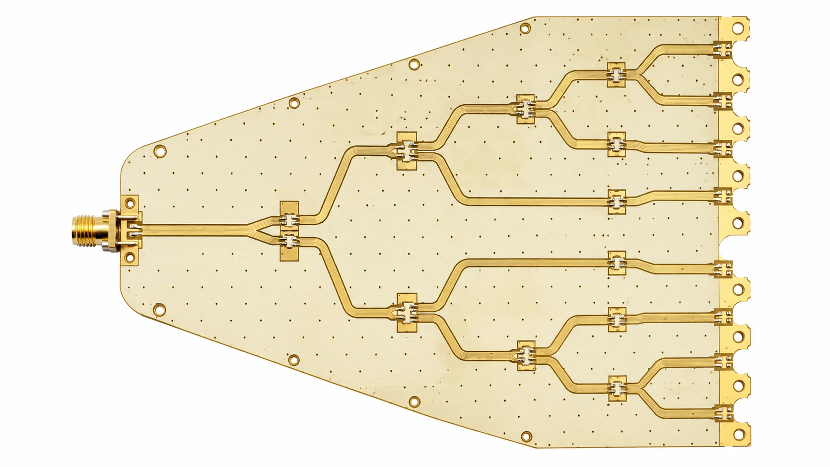
Corporate Feed Network
The most common feed architecture for phased arrays is the corporate (parallel) feed network — a binary tree of power dividers distributing RF signal from a single input to all antenna elements with equal path length. For Ka-band arrays, Wilkinson power dividers in microstrip are standard. Equal path length from input to each element ensures phase uniformity independent of substrate Dk variation — the path length error, not Dk, determines phase accuracy in a corporate feed.
Series Feed Network
Series feed networks route RF along a single transmission line with each element tapping off in sequence. Simpler to implement but frequency-sensitive — phase shift to each element changes with frequency, limiting instantaneous bandwidth. Used primarily for narrow-band arrays where bandwidth requirements are below 5%.
Active Phased Array (AESA)
Active phased arrays integrate T/R (transmit/receive) modules or beamforming ICs directly on the PCB, with individual phase and amplitude control per element. The PCB stackup must support both RF signal distribution and DC power delivery to hundreds of active devices. Multi-layer hybrid stackups with PTFE signal layers and FR4 power/ground layers are standard for AESA designs.
Stackup Design for Phased Array PCB
2-Layer (Simple patch array, passive)
- Top copper: 0.5–1 oz — antenna elements and feed network
- RO3003 core: 0.127 mm (Ka-band) or 0.254 mm (Ku-band)
- Bottom copper: 1 oz — ground plane
4-Layer Hybrid (AESA with integrated beamforming)
- L1 — RO3003 0.127 mm — antenna elements
- L2 — Ground plane
- FR4 prepreg — DC power distribution
- L3 — Power plane
- FR4 prepreg
- L4 — RO3003 0.127 mm — RF feed network
See FR4 + Rogers hybrid PCB stackup guide for bondply selection and press cycle constraints for hybrid AESA stackups.
Manufacturing Requirements
Dk Uniformity Verification
For phased array PCB, request Dk uniformity verification across the panel — not just nominal Dk from the material certificate. Rogers RO3003 material specification guarantees Dk of 3.0 ±0.04 across a panel. Verify that your fabricator performs incoming material inspection and can provide Dk uniformity data for the specific material lot used in your order.
PTFE Plasma Activation
All PTFE phased array substrates (RO3003, RT5880, Taconic, F4B) require in-house plasma activation before copper plating. For phased array applications where the board operates in thermal cycling environments, the adhesion quality of copper on PTFE hole walls is critical — outsourced plasma activation introduces process control risk. See PTFE PCB manufacturing challenges for full process detail.
Impedance Control
Request ±5% impedance tolerance with TDR verification at multiple locations across the panel — minimum 5 measurement points for panels larger than 200 × 200 mm. This confirms Dk uniformity translates into impedance uniformity across all antenna elements. Standard single-point TDR on edge coupons is not sufficient for phased array applications. See controlled impedance RF PCB for full TDR specification guidance.
Dimensional Accuracy
Patch antenna element dimensions determine resonant frequency — for a Ka-band patch at 28 GHz, the element dimension is approximately 3.5 mm on RO3003. A dimensional error of ±0.05 mm shifts resonance by approximately 400 MHz. Specify dimensional tolerance on the fabrication drawing and confirm your fabricator’s etching accuracy at the required line width.
Applications
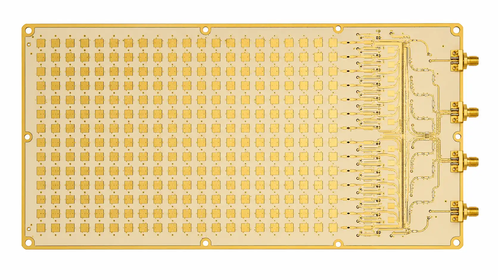
- AESA radar — airborne fire control, ground-based air defense, naval radar
- 5G mmWave massive MIMO base station antenna PCB — 64T64R arrays
- LEO satellite user terminal — Starlink, OneWeb, Kuiper Ka-band phased array
- Electronic warfare — wideband ESM phased array receiver
- Automotive radar — 77 GHz MIMO radar front-end array
- 5G FWA CPE — fixed wireless access customer premise equipment
- Missile seeker — Ka-band active seeker phased array
Conclusion
Phased array PCB requires PTFE substrate with tight Dk uniformity across the panel (±0.05), ±5% impedance control verified at multiple panel locations, in-house plasma activation, and ENIG surface finish for dimensional accuracy. Rogers RO3003 is the standard for most Ka-band and 5G mmWave phased arrays; RT5880 for wideband and lowest-loss applications; RO4350B for S-band and C-band passive arrays. Riching PCB manufactures phased array PCB with RO3003, RT5880, and RO4350B in stock, in-house plasma activation, panel-level TDR verification available, no MOQ. See high frequency PCB capabilities for full factory specifications.
Get a Quote for Your Phased Array PCB
RO3003, RT5880 and RO4350B in stock. In-house plasma activation. Panel-level TDR available. Send the following for DFM review:
- Gerber files + NC drill file
- Array frequency and application type
- Material grade and dielectric thickness
- Stackup drawing — layer count and copper weight
- Impedance tolerance required (±10% or ±5%)
- Panel-level TDR verification required? (yes/no)
- IPC Class and quantity
WhatsApp +86 13760473650 — DFM review within 24 hours
Phased Array PCB Q&A
Common questions about phased array PCB including material selection, Dk uniformity requirements, impedance verification, lamination limits and prototype lead times.
What material is used for phased array PCB?
RO3003 (Dk 3.0, Df 0.0010) is standard for Ka-band and 5G mmWave arrays — tight Dk tolerance ±0.04, stable over temperature. RT5880 (Dk 2.20, Df 0.0009) for wideband and lowest-loss applications. RO4350B for S-band and C-band passive arrays below 8 GHz.
Why is Dk uniformity across the panel critical for phased array PCB?
Dk variation shifts resonant frequency and electrical path length of individual elements, creating phase errors between elements. At 28 GHz, ±0.05 Dk variation shifts patch resonance by 300–400 MHz and introduces beam steering errors. Dk uniformity across the panel — not just nominal Dk — is the critical specification.
What impedance verification is required for phased array PCB?
±5% impedance tolerance, TDR at multiple panel locations — minimum 5 points for panels over 200×200 mm. Single-point edge coupon TDR is not sufficient. Request panel-level TDR verification explicitly on the fabrication drawing.
What is the maximum lamination cycles for PTFE phased array PCB?
Maximum 2 press cycles for all PTFE materials (RO3003, RT5880, Taconic, F4B). Exceeding this causes PTFE deformation and Dk variation across the panel, directly degrading phased array beam performance. Multi-layer AESA designs use hybrid PTFE + FR4 stackups with Rogers bondply.
What is the prototype lead time for phased array PCB?
RO4350B S/C-band: 5–7 working days. RO3003 / RT5880 Ka-band PTFE: 7–10 working days. Panel-level TDR available on request. No MOQ — from 1 board. WhatsApp: +86 13760473650.
Request a PCB Quote
Upload your Gerber ZIP file and project requirements. Our engineering team will review your PCB material, stackup, impedance needs, surface finish, and production quantity before quoting.
Please prepare:
- Gerber files in ZIP format
- PCB material or stackup requirements
- Controlled impedance notes if available
- Prototype or batch production quantity
