
77GHz Radar PCB Design Guide — Patch Array, Via Fence and Stackup Rules
77GHz FMCW radar PCB design operates at the edge of what conventional PCB fabrication tolerances can reliably support — element spacing under 2mm, trace widths under 0.3mm, and via fence spacing tight enough to require laser drilling. This guide covers the practical design rules: patch antenna element spacing, via fence design for parallel-plate mode suppression, 50Ω trace width on Rogers RO3003, and stackup design for hybrid RF/digital automotive radar boards. For material selection background, see 77GHz radar PCB manufacturer.
Home » 77GHz Radar PCB Design Guide — Patch Array, Via Fence and Stackup Rules
Table of Contents
Why RO3003 0.127mm Is the Standard Substrate
At 77GHz, substrate choice is constrained by two factors simultaneously: insertion loss and trace geometry. Rogers RO3003 (Dk 3.0, Df 0.0010) at 0.127mm thickness produces a 50Ω trace width of approximately 0.28mm with 0.5oz copper — narrow enough to support λ/2 patch element spacing (~1.95mm) without the feed network overlapping adjacent elements. RO4350B at the same thickness produces a wider trace and substantially higher insertion loss (~1.4 dB/cm at 77GHz vs ~0.35 dB/cm for RO3003) — making it unsuitable for this application regardless of trace width considerations.
Patch Element Spacing
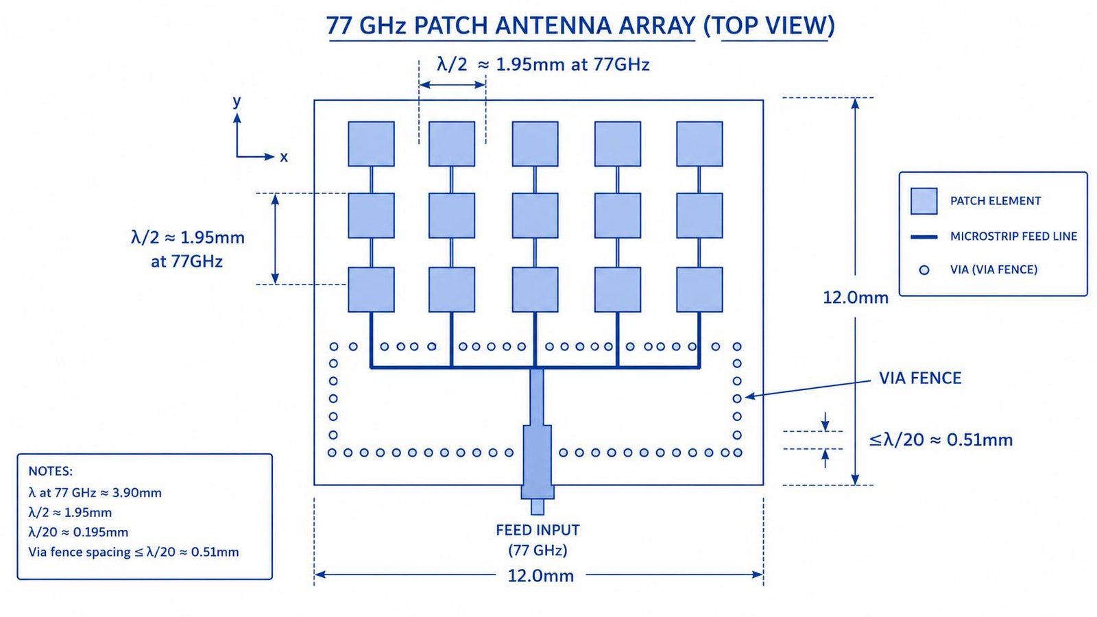
Standard patch array design targets λ/2 element spacing to avoid grating lobes in the antenna pattern. At 77GHz on RO3003 (effective Dk accounting for fringing fields, approximately 2.7–2.8), the guided wavelength is approximately 3.9mm, giving a target element spacing near 1.95mm. This spacing must accommodate both the patch element dimension itself and the feed line routing between elements — at 0.127mm substrate with ~0.28mm trace width, there is limited but workable room for the feed network within this pitch.
Via Fence Design for Ground Isolation
| Parameter | Value at 77GHz | Design Note |
|---|---|---|
| Via fence spacing target | ≤λ/20 ≈ 0.51mm | Stricter than lower-frequency designs — requires laser-drilled microvias |
| Via drill diameter | 0.1mm laser drill | Mechanical drilling (0.2mm) too coarse for fence spacing at this frequency |
| Via-to-trace edge clearance | ≥3× trace width | Prevents fence proximity from perturbing feed line impedance |
| Ground via stitching near connector transitions | Continuous ring, ≤λ/20 | Critical at SMA/waveguide transitions to suppress parallel-plate modes |
Via fences suppress parallel-plate waveguide modes that can propagate between ground and signal layers, particularly important around antenna feed transitions and connector interfaces. The standard design guideline targets via spacing at or below λ/20 to effectively present a continuous ground wall at the operating frequency. At 77GHz, this works out to approximately 0.51mm spacing — fine enough that mechanical drilling (typically 0.2mm minimum diameter, larger practical spacing) cannot achieve the required density. Laser-drilled microvias (0.1mm diameter) are required for via fence implementation at this frequency.
Stackup Design for Hybrid 77GHz Radar Boards
| Layer Function | Typical Material | Design Note |
|---|---|---|
| RF top layer (patch array + feed) | RO3003 0.127mm | Element spacing ~1.95mm at 77GHz, 0.5oz copper, ENIG |
| Ground reference | RO3003 (same panel) | Continuous ground directly beneath RF layer — no splits under feed lines |
| Transition/bonding layer | Rogers 2929 bondply | Required at RO3003-to-FR4 interface — not standard prepreg |
| Digital/control layers | FR4 or Hi-Tg FR4 | Signal processing, power, MCU/SoC interconnect |
| Backdrill layer (if applicable) | — | Remove via stub on transitions between RF and digital layers |
Most automotive 77GHz radar designs combine an RF front-end (antenna array and feed network on RO3003) with digital signal processing layers (FR4 or Hi-Tg FR4) in a single hybrid stackup — reducing system cost compared to an all-Rogers board while keeping RF performance on the critical layers. The bonding interface between RO3003 and FR4 requires Rogers 2929 bondply, not standard FR4 prepreg — using the wrong bonding film at this interface introduces both a reliability risk and an impedance discontinuity. See Rogers RO3003 PCB manufacturer for hybrid stackup material availability.
Via Stub and Backdrill Considerations
In a hybrid stackup where the RF layer sits on the outer layers and digital signal vias pass through the full board thickness, unused via stub length can create resonant notches in the transmission response. At 77GHz, even a short stub (sub-millimeter) can produce a notch within or near the operating band depending on stub length and substrate Dk. For transitions where via stub length cannot be kept negligibly short by design, backdrill should be specified to remove the unused stub portion.
DFM Checklist for 77GHz Radar PCB
| DFM Check Item | 77GHz-Specific Requirement |
|---|---|
| Substrate thickness and Dk tolerance | 0.127mm RO3003, Dk 3.0 ±0.04 — confirm panel-level Dk uniformity for array phase consistency |
| Trace width verification | ~0.28mm for 50Ω at 0.127mm/0.5oz — verify against actual Dk certificate, not nominal |
| Via fence spacing | ≤0.51mm (λ/20) — confirm laser drill capability, not mechanical |
| Element spacing tolerance | ±0.02mm typical — confirm etching tolerance supports this at panel scale |
| Surface finish flatness | ENIG — flat surface required for dimensional accuracy of patch elements |
| Backdrill specification (if hybrid stackup) | Confirm stub length target and depth control tolerance with fabricator |
Common Design Errors at 77GHz
- Specifying mechanical drill for via fence — at 77GHz spacing requirements, mechanical drilling cannot achieve adequate fence density. Specify laser drill explicitly.
- Using nominal Dk instead of measured Dk from material certificate — at 0.127mm substrate, small Dk variation produces proportionally larger trace width and impedance error than at thicker substrates.
- Splitting ground plane directly beneath the feed network — any ground discontinuity beneath a 77GHz feed line creates significant return loss degradation.
- Underspecifying element-to-element etching tolerance — patch array phase consistency depends on dimensional consistency across the panel, not just nominal element size.
- Treating via stub as negligible without checking stub length against λ/4 at 77GHz — what is negligible at lower frequencies may not be at mmWave.
77GHz Radar PCB Design — Q&A
Common questions about patch antenna element spacing, via fence design, trace width on RO3003, and stackup considerations for 77GHz automotive radar PCB.
What is the patch element spacing for 77GHz radar antenna design?
Standard patch array design targets λ/2 element spacing to avoid grating lobes. At 77GHz on RO3003 (effective Dk ~2.7-2.8), the guided wavelength is approximately 3.9mm, giving a target element spacing near 1.95mm.
Why does 77GHz radar PCB require laser-drilled via fence instead of mechanical drilling?
Via fence spacing at 77GHz should be at or below λ/20, approximately 0.51mm. Mechanical drilling (minimum ~0.2mm with larger spacing) cannot achieve this density. Laser-drilled microvias (0.1mm) are required for an effective fence at this frequency.
What is the 50Ω trace width for 77GHz radar PCB on RO3003?
On RO3003 at 0.127mm with 0.5oz copper, the 50Ω trace width is approximately 0.28mm — narrow enough to fit within the λ/2 element spacing. Always verify against the actual Dk from the material certificate, not nominal datasheet values.
What bonding film is used for 77GHz radar hybrid stackups?
Rogers 2929 bondply is required at the RO3003-to-FR4 interface. Standard FR4 prepreg should not be used — it creates dimensional and Dk discontinuities affecting both reliability and electrical performance.
RO3003 0.127mm In Stock — Laser Drill Via Fence Capable
77GHz radar PCB fabrication with laser-drilled microvias for fence spacing, ENIG finish, Rogers 2929 bondply for hybrid stackups. IATF16949 certified. 7–10 day prototype, no MOQ.
77GHz Radar PCB Manufacturer → WhatsAppRequest a PCB Quote
Upload your Gerber ZIP file and project requirements. Our engineering team will review your PCB material, stackup, impedance needs, surface finish, and production quantity before quoting.
Please prepare:
- Gerber files in ZIP format
- PCB material or stackup requirements
- Controlled impedance notes if available
- Prototype or batch production quantity