
EW PCB Wideband Design Guide — Material Selection, Stub Length and Loss Budget Across 2–18GHz
Electronic warfare PCB design presents a constraint that most RF designs don't face: the same board must perform consistently across a very wide instantaneous bandwidth — often 2–18GHz or wider — rather than a narrow band centered on a single operating frequency. This changes the design priorities: material loss at the highest frequency in the band matters as much as the band center, impedance must hold across the full sweep, and via stub resonances that would be irrelevant in a narrowband design can fall directly inside a wideband passband. This guide covers the practical design considerations specific to wideband EW PCB. For material stock and stackup options, see EW PCB manufacturer.
Home » EW PCB Wideband Design Guide — Material Selection, Stub Length and Loss Budget Across 2–18GHz
Table of Contents
Material Selection Across EW Bands
| Band | Frequency Range | Common EW Function | Material Priority |
|---|---|---|---|
| S/C band | 2–6 GHz | Wideband ESM, jammer front-end | Lowest Df across band — RT5880 |
| X band | 6–12 GHz | Fire control radar intercept, X-band ESM | RT5880 or RT5870 depending on layout density |
| Ku band | 12–18 GHz | SATCOM intercept, fine-resolution ESM | RT5880, verify loss budget margin |
| Multi-octave (2–18GHz) | 2–18 GHz | DRFM input, wideband digital receiver front-end | RT5880 — single material across full band simplifies stackup |
Rogers RT5880 (Dk 2.20, Df 0.0009) is the standard material for wideband EW design because it offers the lowest Df among readily available materials, and Df is the parameter that determines insertion loss across the entire band — not just at one frequency point. See RT5880 vs RT5870 vs RO3003 for a detailed comparison of when each material is the better choice.
Loss Budget Across the Band
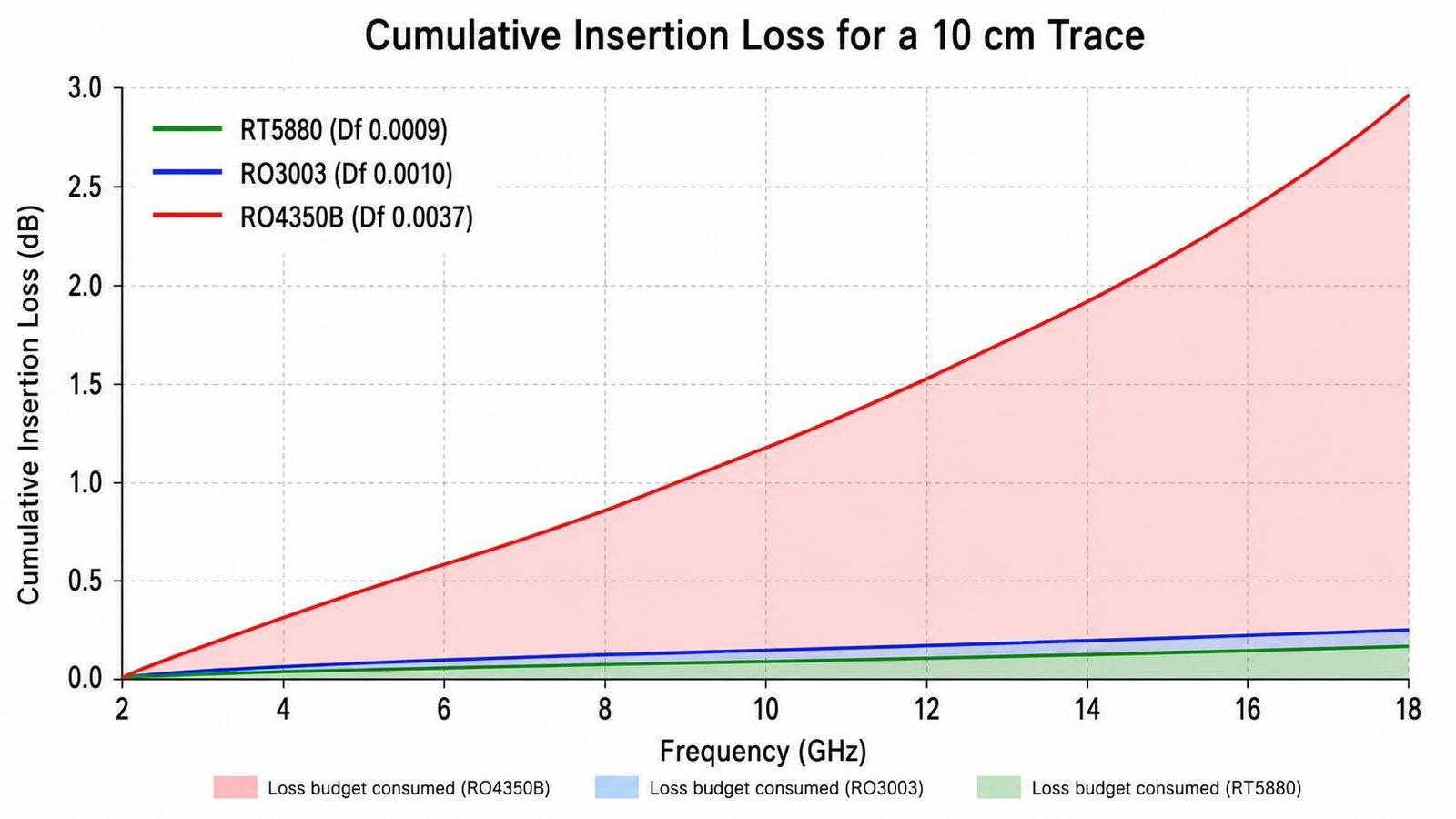
| Trace Length | RT5880 (Df 0.0009) | RO3003 (Df 0.0010) | RO4350B (Df 0.0037) |
|---|---|---|---|
| 5cm @ 6GHz | ~0.18 dB | ~0.20 dB | ~0.66 dB |
| 10cm @ 6GHz | ~0.35 dB | ~0.39 dB | ~1.32 dB |
| 5cm @ 18GHz | ~0.35 dB | ~0.40 dB | ~1.40 dB |
| 10cm @ 18GHz | ~0.70 dB | ~0.80 dB | ~2.80 dB |
Via Stub Management Across a Wide Band
The key design principle for wideband EW: insertion loss scales with frequency, so your loss budget must be evaluated at the highest frequency in your instantaneous bandwidth, not the band center. A design with a 6GHz center frequency but 2–12GHz instantaneous bandwidth needs its loss budget verified at 12GHz, where insertion loss is roughly double what it is at 6GHz. Designs that pass simulation at center frequency but were never checked at the band edge are a common source of post-fabrication performance shortfall.
Via Stub Management Across a Wide Band
- Single-section matching networks rarely hold acceptable return loss across a full octave or more — multi-section matching (Chebyshev or similar) is typically required for 2–18GHz designs
- Coupled-line and Lange couplers used in wideband power dividers are sensitive to Dk tolerance — confirm material Dk tolerance (RT5880 typically ±0.02 to ±0.04 depending on grade) supports your coupling accuracy requirement
- Wideband baluns and transformers benefit from RT5880’s lower Dk — physically larger structures are sometimes easier to fabricate with tighter dimensional control than the equivalent RO3003 design at the same impedance
Design Checklist for Wideband EW PCB
| DFM/Design Check Item | Wideband EW-Specific Requirement |
|---|---|
| Material selection | Confirm Df is acceptable at the highest frequency in the instantaneous band, not just band center |
| Trace impedance vs frequency | Verify 50Ω holds across full bandwidth — wideband designs more sensitive to Dk dispersion |
| Via stub length | Calculate λ/4 notch frequency at highest operating frequency — backdrill if notch falls within band |
| Connector transition | Verify SMA/2.92mm launch optimized across full bandwidth, not just one frequency point |
| TDR impedance tolerance | Specify ±5% for wideband designs — tighter tolerance reduces return loss ripple across band |
| Material lot consistency | For multi-board systems, request single-lot material to minimize element-to-element Dk variation |
Stackup and Process Notes
- RT5880 requires in-house plasma activation — same PTFE process requirements as RO3003
- Maximum 2 lamination press cycles for RT5880 — applies to the full stackup if hybrid construction is used
- For multi-element systems (array feeds, multi-channel receivers), request single-lot material across all boards to minimize Dk variation between elements
- TDR verification at multiple frequency points across the band — a single-frequency TDR check does not confirm wideband impedance consistency
EW PCB Wideband Design — Q&A
Common questions about material selection, loss budget calculation, via stub management and impedance tolerance for wideband EW PCB across 2–18GHz.
What material is best for wideband EW PCB design?
Rogers RT5880 (Dk 2.20, Df 0.0009) is the standard material, offering the lowest dissipation factor among commonly available substrates. Since Df determines loss across the entire instantaneous bandwidth, RT5880's low loss is consistent whether the design operates at 2GHz or 18GHz.
Why does loss budget matter more at the highest frequency in a wideband design?
Insertion loss scales with frequency, so loss budget must be evaluated at the highest frequency in the instantaneous bandwidth, not the band center. A 2-12GHz design needs its budget checked at 12GHz, where loss is roughly double what it is at 6GHz.
Why is via stub management harder for wideband EW PCB?
Via stubs create a notch at λ/4. In narrowband designs this notch can be placed outside the operating band. In a 2-18GHz wideband design, there is much less safe frequency space — a stub resonating at 14GHz falls directly inside the band, requiring backdrill or via structure changes.
What TDR tolerance is recommended for wideband EW PCB?
±5% TDR tolerance is recommended over the standard ±10%, because tighter impedance control reduces return loss ripple across the full bandwidth. TDR should be verified at multiple frequency points, not just a single check point.
RT5880 In 6 Thicknesses — Lowest Df for Wideband EW
Full thickness range in stock (0.127mm–1.575mm). In-house plasma activation. Single-lot material available for multi-channel array systems. IPC Class 3 on request. 7–10 day prototype, no MOQ.
EW PCB Manufacturer → WhatsAppRequest a PCB Quote
Upload your Gerber ZIP file and project requirements. Our engineering team will review your PCB material, stackup, impedance needs, surface finish, and production quantity before quoting.
Please prepare:
- Gerber files in ZIP format
- PCB material or stackup requirements
- Controlled impedance notes if available
- Prototype or batch production quantity
Via stubs create a notch in transmission response at the frequency where stub length equals λ/4. In a narrowband design, this notch can often be placed safely outside the operating band. In a wideband design spanning 2–18GHz, the available ‘safe’ frequency space for a stub notch shrinks dramatically — a stub that resonates at 14GHz sits directly inside the operating band of a 2–18GHz receiver, with no way to move it outside the band without changing the physical via structure.
For wideband EW designs, the practical approach is usually to minimize via stub length by design wherever the through-hole via passes through layers not used by the RF signal, and to specify backdrill on any via where stub length cannot be controlled by stackup design alone. Calculate the stub resonance frequency for your actual stub length and confirm it falls outside your full instantaneous bandwidth — not just outside the band center.