
Low-Noise Amplifier PCB Design — Grounding, Shielding and Layout Rules for Minimum Noise Figure
A low-noise amplifier's datasheet noise figure is achieved only under the specific source and ground conditions the manufacturer tested against — the PCB around the device is not a passive carrier, it is an active contributor to the system's actual noise performance. Every dB of insertion loss ahead of the LNA adds directly to system noise figure, and ground via inductance under the device can degrade both gain and noise performance below datasheet values. This guide covers the PCB-specific grounding, shielding, and layout considerations that determine whether an LNA stage actually delivers its rated noise figure once built.
Home » Low-Noise Amplifier PCB Design — Grounding, Shielding and Layout Rules for Minimum Noise Figure
Table of Contents
Noise Figure Budget — Where the PCB Contributes
| Noise Contribution Source | Typical Impact on NF | PCB Layout Mitigation |
|---|---|---|
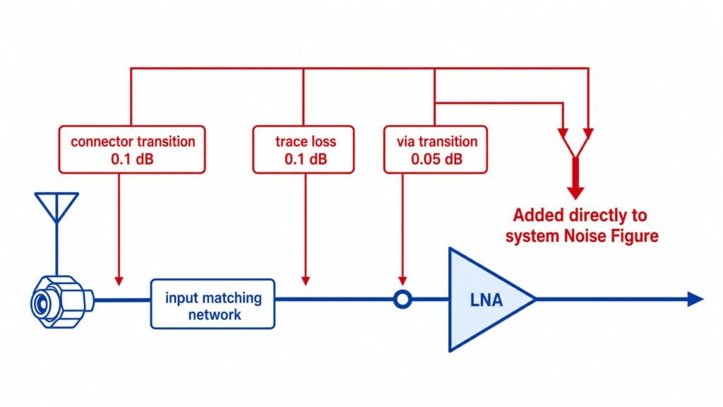
| Input matching network insertion loss | Adds directly to NF, dB-for-dB | Minimize trace length, low-Df substrate, minimize via count |
| Ground via inductance under LNA | Degrades gain and can add noise via feedback | Maximize via count, minimize length, copper fill preferred |
| Power supply noise coupling into bias network | Modulates LNA gain/noise if unfiltered | Dedicated low-noise supply routing, decoupling close to device |
| Digital switching noise coupling into RF section | Raises noise floor, can appear as spurious tones | Physical separation, ground via fence isolation |
| Connector/cable transition loss before the LNA | Adds directly to system NF | Minimize transition loss |
The cascade noise figure formula means the first gain stage — and everything ahead of it — dominates system noise performance. Any insertion loss in the input matching network, connector transition, or trace between the antenna and the LNA input adds to system NF at essentially 1:1, because it occurs before any gain has been applied to overcome it. This is why input-side PCB losses matter disproportionately more than losses anywhere else in the receive chain, and why material and layout choices ahead of the LNA deserve more attention than equivalent choices later in the signal path.
Grounding Requirements Specific to LNA Stages
| Grounding Element | Requirement | Why It Matters for LNA |
|---|---|---|
| Ground via count under device package | Maximize within footprint, per datasheet | Parallel vias reduce total ground inductance |
| Ground via fill type | Copper fill preferred | Lower inductance than resin fill |
| Ground plane continuity under input trace | No splits or gaps, ever | Discontinuity raises effective source impedance |
| Shielding can grounding | Continuous solder contact, not just corner tabs | Gaps leak interference into the most sensitive stage |
| Bias/control line ground reference | Adequate stitching vias near transitions | Prevents control line acting as unintended antenna |
Ground via inductance under the LNA package behaves similarly to the thermal via considerations covered in our GaN PA thermal design guide — dense, copper-filled via arrays reduce inductance — but for an LNA the primary concern is noise and gain performance rather than thermal dissipation, since LNAs typically dissipate far less power than a PA stage. The via array requirement is driven by RF ground reference quality, not heat removal.
Shielding Can Layout
Many LNA and receiver front-end designs specify a metal shielding can over the sensitive stage to block external interference. The can’s effectiveness depends entirely on ground continuity around its perimeter — a shielding can with gaps in its ground contact provides significantly less isolation than the can’s specification suggests, because RF energy leaks through any discontinuity in the ground path rather than being blocked by the can material itself. Specify continuous solder contact around the can perimeter footprint, not just corner tabs, and verify this is achievable with your fabricator’s solder mask and pad design before finalizing layout.
Power Supply and Control Line Isolation
Power supply noise reaching the LNA’s bias network can modulate the device’s gain or noise performance, appearing as unwanted sidebands or a raised effective noise floor. Route the LNA’s DC supply separately from any digital switching supply rail where practical, and place decoupling capacitors as close to the device as the layout allows. Digital control lines near the LNA — enable/disable, gain control on variable-gain devices — should be treated as potential noise sources and isolated with the same ground via fence approach used to separate RF from digital sections generally.
Material Selection for the LNA Input Path
| Material | Dk | Df | LNA Input Path Suitability |
|---|---|---|---|
| Rogers RT5880 | 2.20 | 0.0009 | Lowest loss — preferred for input matching network |
| Rogers RO3003 | 3.0 | 0.0010 | Comparable loss, higher via density tolerance |
| Rogers RO4350B | 3.48 | 0.0037 | Acceptable below ~6GHz where loss budget allows |
Because input-side loss adds directly to noise figure, material selection ahead of the LNA deserves the lowest-Df option that fits the design’s frequency and cost constraints. See our Rogers RT5880 PCB guide and Rogers RO3003 PCB guide for the property comparison that applies directly to input matching network material selection.
DFM Checklist for LNA Front-End PCB
- Confirm ground via count and fill type under the LNA package against the device’s datasheet recommendation, not a generic RF via pattern
- Specify continuous shielding can ground contact around the full perimeter, not just corner tabs
- Minimize trace length and via count in the input matching network — every element ahead of the LNA adds to system NF
- Confirm connector launch geometry ahead of the LNA follows the same tolerance rules as any RF connector transition — see our RF connector launch design guidefor launch geometry specifics
- Route DC bias and control lines with dedicated ground stitching, physically separated from the RF signal path
LNA PCB Grounding and Shielding — Q&A
Common questions about noise figure budget, ground via requirements, and shielding can layout for LNA front-end PCB.
Why does PCB layout affect LNA noise figure?
Any insertion loss ahead of the LNA — input matching network trace, connector transition, via — adds directly to system noise figure at essentially 1:1, since it occurs before any gain stage can overcome it. Ground via inductance under the device also degrades gain and noise performance if not controlled.
What ground via requirements apply to LNA package footprints?
Maximize ground via count per datasheet, using copper-filled vias for lower inductance. Driven by RF ground reference quality rather than thermal dissipation, since LNAs dissipate far less power than a PA stage.
Why does shielding can grounding matter for LNA designs?
Shielding effectiveness depends entirely on ground continuity around the perimeter. Gaps allow RF energy to leak through, providing much less isolation than specified. Continuous solder contact around the full perimeter is required.
LNA Front-End PCB — Ground Via Arrays and Shielding Verified at DFM
Copper-filled ground vias under LNA packages, continuous shielding can ground pattern review, Rogers RT5880 and RO3003 in stock for lowest input-path loss. Connector launch DFM review included.
RF Front-End PCB Design → WhatsAppRequest a PCB Quote
Upload your Gerber ZIP file and project requirements. Our engineering team will review your PCB material, stackup, impedance needs, surface finish, and production quantity before quoting.
Please prepare:
- Gerber files in ZIP format
- PCB material or stackup requirements
- Controlled impedance notes if available
- Prototype or batch production quantity