
Corporate Feed Network PCB: Series vs Parallel Feed, Quarter-Wave Transformers and Loss Budget
Corporate feed network PCB design: series vs parallel feed, quarter-wave transformer impedances, amplitude taper, loss budget and the etch tolerances behind it.
Home » Antenna PCB » Corporate Feed Network PCB: Series vs Parallel Feed, Quarter-Wave Transformers and Loss Budget
Table of Contents
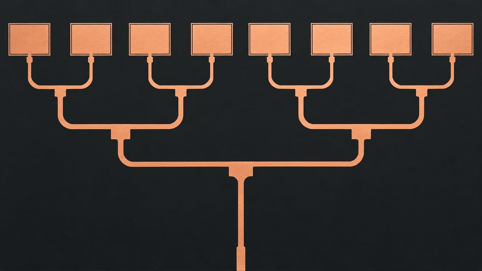
A corporate feed network is the branch-and-junction structure that splits RF power from one port to the elements of a planar antenna array — or combines their returns into one port. It is called corporate because the tree diagram of junctions resembles an organisation chart: one input at the top, a defined split at every level, every element reachable by a path of the same electrical length.
That last property is the whole point. Because every element sits behind the same number of junctions, the network holds a defined amplitude and phase relationship across the array — which is what keeps the beam pointing where the drawing says, and what lets a low-sidelobe amplitude taper be set per element rather than left to the physics of a loaded line.
This page covers the two feed families and what each trades away, the quarter-wave transformer arithmetic that fixes the section impedances, a computed λg/4 length table, the loss budget of a real split, the layout rules that keep junctions honest, and the fabrication tolerances that decide whether the built network matches the simulated one. Array-level context sits in our phased array PCB review, and the geometry-driven design view is in the phased array PCB design guide.
1. What a Corporate Feed Network Is
Every corporate network is built from three primitives: a 50 ohm feed line, a power-splitting junction, and a quarter-wave impedance transformer in each arm that makes the split come out right. Nothing else is required — no components, no resistors, no tuning elements. The entire network is copper geometry, which is why it is cheap to replicate and predictable to build.
The predictability is the design asset. A series feed loads its line progressively, so element after element sees a different impedance and the amplitudes are set by the loading schedule; a corporate feed isolates each junction from the rest of the tree, so each split can be designed and verified on its own. When an antenna has a sidelobe requirement, that modularity is what makes the taper achievable at all.
The cost is area and loss. A corporate network spreads across the board behind the elements, and every junction and transformer section adds a little insertion loss and a little phase error. On a 1:8 network that overhead is small; on a 1:64 planar array it becomes a design exercise in its own right, which is where the layout discipline in the later sections earns its keep.
2. Series vs Parallel Feed: What Each Structure Trades
The two feed families answer the same problem with opposite priorities. The table sets the differences out as design consequences rather than as a ranking:
| Aspect | Corporate (parallel) feed | Series (travelling-wave) feed |
|---|---|---|
| Path from input to element | Every element sits behind the same number of junctions | Elements tap one progressively loaded line |
| Phase behaviour vs frequency | Each arm is electrically symmetric — the beam points where the network says, at any frequency in band | Progressive phase shifts with frequency — the beam squints off boresight as frequency moves |
| Amplitude control | Set per element by the divider ratios — arbitrary tapers including low-sidelobe windows | Set by coupling along the line — taper is constrained by the loaded-line design |
| Loss mechanism | Splitter junctions + transformer sections + line loss | Residual power absorbed in the termination at the far end |
| Port isolation | None between output ports (that is a Wilkinson divider, which adds resistors) | None; coupling is through the line itself |
| Typical use | Base station panels, GNSS patches, planar arrays where the beam must not squint | Slots and series patches where the squint is budgeted or the band is narrow |
Parameter facts only. Both structures appear on production antennas; the choice is made on squint budget and taper requirement, not on which one is "better".
The squint row is the one that decides most programmes. A series-fed array that must hold pointing accuracy across a wide band needs its squint budgeted and compensated; a corporate-fed array does not squint by construction, because no element is deeper in the network than any other. Amplitude taper is the second decider — sidelobe masks are set per element, and per-element control is native to the corporate form.
3. The Quarter-Wave Transformer: Arithmetic That Fixes the Geometry
A quarter-wave section of characteristic impedance ZT transforms a load ZL into an input of ZT²/ZL. Every impedance in a corporate network follows from that one relation. At a junction that must combine its arms back to 50 ohms, each arm has to present 100 ohms, and the section that gets there from a 50 ohm port is the geometric mean:
| Split | Each arm must present at the junction | Quarter-wave transformer per arm |
|---|---|---|
| 1 : 2, all ports 50 Ω | 100 Ω (two in parallel = 50 Ω) | √(50 × 100) = 70.7 Ω |
| 1 : 3, all ports 50 Ω | 150 Ω (three in parallel = 50 Ω) | √(50 × 150) = 86.6 Ω |
| 1 : 4, two levels of 1 : 2 | 100 Ω at every junction | 70.7 Ω — six identical sections |
| 1 : 8, three levels of 1 : 2 | 100 Ω at every junction | 70.7 Ω — fourteen identical sections |
The structural insight: with equal power split and 50 Ω everywhere, every junction combines two or more 100 Ω arm impedances back to 50 Ω, so every quarter-wave section in the tree has the same characteristic impedance no matter how many levels the network has.
Two practical notes. First, the 86.6 ohm three-way case is rarer than the two-way cascade not because it is worse but because three-way junctions are harder to lay out symmetrically on a rectangular panel. Second, the section count grows quickly — fourteen transformer sections in a 1:8 tree — and every one of them is a place where etch tolerance and bend treatment become electrical errors. That is why section impedance is quoted here to three figures: it is a manufactured dimension, not a concept.
4. Section Length: A Computed λg/4 Table
Transformer length is λg/4 — a quarter of the guided wavelength, not the free-space one. Because the 70.7 ohm section is narrower than the 50 ohm feed, it carries more of its field in air and its effective permittivity is lower, so the section is longer than a quarter-wave of the feed line at the same frequency. The table below gives both, computed for the most common antenna-panel case:
| Frequency | Free-space λ₀ | λg / 4 on a 50 Ω line (mm) | λg / 4 on a 70.7 Ω section (mm) |
|---|---|---|---|
| 3.5 GHz | 85.7 mm | 14.74 | 15.37 |
| 5.8 GHz | 51.7 mm | 8.90 | 9.28 |
| 10 GHz | 30.0 mm | 5.16 | 5.38 |
| 24 GHz | 12.5 mm | 2.15 | 2.24 |
| 28 GHz | 10.7 mm | 1.84 | 1.92 |
Computed values, not estimates transcribed from a datasheet. Assumptions stated in full: microstrip on εr = 2.55, dielectric thickness 0.762 mm; the 50 Ω line solves to W ≈ 2.15 mm with εeff = 2.11, the 70.7 Ω section to W ≈ 1.28 mm with εeff = 1.94 (Wheeler synthesis + Schneider dispersionless formula). The two columns differ because the narrower transformer line carries more of its field in air.
The assumption set matters more than the fourth decimal place. The computation uses microstrip on εr 2.55 and 0.762 mm dielectric — a standard antenna-laminate build. Change the dielectric thickness and both the widths and the effective permittivities move; change material and everything above is the wrong table. The widths themselves are the cross-check worth doing on any quoted stackup: a 50 ohm line solving to 2.15 mm on a 0.762 mm core is the number a layout tool should reproduce before the artwork is trusted.
Impedance targets and the line widths they produce are treated in detail in our 50 ohm RF trace guide, and the tolerance discussion continues in the controlled impedance RF PCB note.
5. Amplitude Taper: What Corporate Feed Makes Possible
A uniform array has a gain problem at the edges of its coverage: the first sidelobes of a uniformly excited aperture sit only about 13 dB down from the main beam. Antenna specifications almost always demand more isolation than that, and the standard answer is to excite the edge elements less — an amplitude taper across the array.
A corporate feed is the structure that makes a taper manufacturable. Because each junction divides power by a chosen ratio, the transformer impedances in each arm can be re-derived to deliver, say, −20 dB or −30 dB Chebyshev-style weighting across the elements, and the whole schedule is fixed in copper at etch time. Nothing is tuned after the fact; the taper is as repeatable as the etch.
The same mechanism cuts the other way. Every ratio change re-derives the transformer impedances, which means the network is no longer a tree of identical 70.7 ohm sections, and each non-standard section is a slightly different width with a slightly different effective permittivity. A tapered network is therefore more sensitive to etch tolerance than a uniform one — which is why the tolerance rows in the manufacturing section matter more on a low-sidelobe array than on a plain splitter.
6. The Loss Budget: Where the Power Actually Goes
The first number in any feed-network loss conversation is the split itself — and it is not loss. Half the ports means half the power, so a 1:2 divider shows 3.01 dB on the network analyser with a perfect component. What matters is everything stacked on top of that floor:
| Loss contribution in a 1 : 8 corporate feed | Value | Where it comes from |
|---|---|---|
| Ideal power split — the floor, not a loss | 9.03 dB | 10·log₁₀(8): half the ports, half the power, at every level |
| Dielectric loss on ≈ 0.35 m of total 50 Ω path @ 3.5 GHz | ≈ 0.18 dB | ≈ 0.52 dB/m computed for εeff 2.11, tanδ 0.0013 (TEM formula with filling-factor correction) |
| Conductor loss on the same path | fraction of a dB | Copper roughness and skin effect; grows with frequency and foil roughness |
| Junction and transformer mismatch | design-dependent | Each λg/4 section is only perfect at its design frequency; steps and uncompensated T-junctions radiate a little |
The split "loss" is thermodynamics, not loss — 9.03 dB of it comes back as gain at the element side. The rows beneath it are the ones a fab drawing can influence. The dielectric figure is a computed worked example on the stated assumptions, not a datasheet value.
Read against a real design, the message is that on a low-loss antenna laminate the split floor dominates and the fabrication overheads are small but systematic. That is exactly why the loss figures in the material datasheet — 0.0013 at 10 GHz on an antenna-grade PTFE laminate such as the grades reviewed in our Arlon high frequency PCB materials overview — are worth the premium on a long feed network: the dielectric term is the only loss row that the material choice controls.
7. Layout Rules: Bends, Junctions and the Ground Around the Network
Between the arithmetic and the finished board sits the layout, and most feed-network surprises are layout surprises. The rules below are the ones that decide whether the built network behaves like the simulation:
| Layout item | Rule of thumb | What goes wrong without it |
|---|---|---|
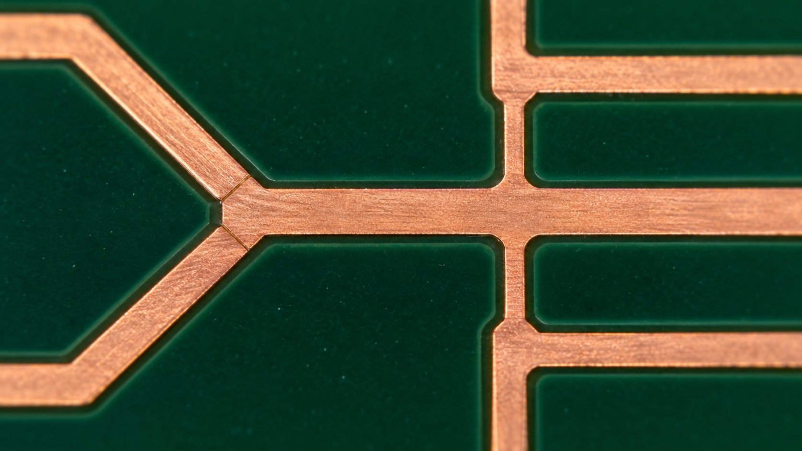
| Right-angle bends | Mitred (chamfered) corners on every 90° turn | Un-mitred corners add a lump of capacitance — a phase and mismatch error at every bend, times every bend |
| T-junctions | Compensate the junction (chamfer or step the branch input) | An uncompensated T presents a reactive discontinuity and can radiate |
| Transformer sections | Keep each λg/4 section clear of other copper; no components over it | Coupling into neighbouring copper perturbs the impedance the section was cut for |
| Symmetry | Mirror the two halves of every split exactly | Asymmetric routing converts an amplitude error into a pointing error |
| Ground stitching | Via fence on λg/10 pitch along the network edges | Ground loops between patches behave like unintended radiators; see the via fence guide |
| Solder mask | Keep mask off the radiating side; declare it on the drawing | Mask over radiating structures shifts resonance and adds loss |
Rules of thumb for planar corporate networks. None of them are optional on a low-sidelobe array; each one converts directly into amplitude or phase error at the elements.
The ground row deserves a note of its own. On a feed network the ground return is part of the transmission line, and stitching it properly is what keeps the return current where the design assumes it to be. Stitch pitch, fence placement and the interaction with radiating elements are worked through in our via fence PCB guide.
8. Manufacturing Tolerances: What the Factory Has to Hold
A feed network converts etch geometry into amplitude and phase, so the fabrication tolerance discussion is an electrical discussion. The rows below are the ones that matter on a production antenna build:
| What the factory holds | Typical capability | Effect on the network |
|---|---|---|
| Trace etch tolerance | ± 15 µm on outer layers is a common RF-grade request | A 70.7 Ω section is only 1.28 mm wide at 0.762 mm dielectric; ± 15 µm is ± 1.2 % of width — a small impedance and amplitude error per section |
| Impedance verification | Coupon TDR against the agreed design Dk | Converts the drawing assumption into a measured number for the lot actually built |
| Copper foil profile | Reverse-treated foil on loss-critical networks | Rougher foil raises conductor loss and, on PIM-limited antennas, the PIM level too |
| Mask and finish on the radiating side | Mask-free radiating areas; finish chosen for loss | Mask and nickel-bearing finishes over radiating copper both cost loss |
Capability rows are stated as common RF-grade requests, not as universal guarantees; the numbers to build against are the ones agreed on your drawing. What matters for a feed network is that the errors are systematic — they repeat on every board, so they are measurable on the coupon and correctable in artwork.
The practical sequence on a new array is short: agree the design Dk and the impedance targets in writing, confirm the dielectric thickness that keeps every transformer section manufacturable, and require coupon TDR data on the build lot. Fabrication of radiating structures and their feeds is described on our antenna PCB page, and the millimetre-wave end of the tolerance discussion — where a 70.7 ohm section is under two millimetres long — continues in the 77 GHz radar PCB design guide and the X/Ku-band AESA radar PCB manufacturing guide.
Corporate Feed Network PCB — Frequently Asked Questions
What the network is, why the transformers are 70.7 Ω, corporate vs series feed, and whether isolation resistors belong in it.
What is a corporate feed network?
A corporate feed network — also called a parallel feed — is the branch-and-junction structure that divides RF power from one input port to the elements of a planar antenna array, or combines their received power into one port. Each element sits behind the same number of junctions, so every element receives the same phase at the design frequency regardless of its position in the array. The junctions are built from quarter-wave impedance transformer sections, which is why the geometry is fully deterministic and can be etched as part of the PCB artwork.
Why is every quarter-wave transformer in a corporate feed 70.7 ohms?
Because of what each junction has to do. With all ports at 50 ohms and an equal power split, the two arms meeting at a junction must each present 100 ohms so that the pair combines back to 50. The quarter-wave section that transforms a 50 ohm port to a 100 ohm junction has a characteristic impedance of the geometric mean, √(50 × 100) ≈ 70.7 ohms. The same logic holds at every junction of the tree, so a 1:4 network uses six identical 70.7 ohm sections and a 1:8 network uses fourteen — only the section lengths change with frequency.
Corporate feed vs series feed: which one should an array use?
The deciding questions are beam squint and amplitude control. A corporate network gives every element the same electrical path length, so the beam does not squint as frequency moves across the band, and element amplitudes can be set independently by the divider ratios — which is what low-sidelobe tapers require. A series feed is shorter and simpler, but its progressive phase shifts with frequency, so the beam squints, and the taper is constrained by the loaded-line design. Narrowband arrays that can budget the squint use series feed; base station panels and anything with a sidelobe mask almost always use corporate.
Does a corporate feed network need isolation resistors?
No — and that distinction is worth keeping sharp. A Wilkinson divider adds a resistor between the two output arms to absorb the difference-mode power, which buys isolation between ports at the cost of an extra component. A plain corporate feed has no resistors: power reflected from one element simply re-enters the network through the junctions. Arrays that need port isolation use Wilkinson structures; arrays that need only a defined split use the corporate form and control the coupling by layout instead.
Building an array with a corporate feed?
Send us the band, the element count and the impedance targets for the feed lines. We will confirm the dielectric thickness that makes the quarter-wave sections manufacturable, hold the etch tolerance the taper needs, and quote fabrication with coupon TDR data on the lot we actually build from.
Contact Us → WhatsApp: +86 137 6047 3650Request a PCB Quote
Upload your Gerber ZIP file and project requirements. Our engineering team will review your PCB material, stackup, impedance needs, surface finish, and production quantity before quoting.
Please prepare:
- Gerber files in ZIP format
- PCB material or stackup requirements
- Controlled impedance notes if available
- Prototype or batch production quantity