
Via Fence in RF PCB: Spacing Rules, Ground Stitching and Layout Examples
Ground via fence design rules for RF PCB — the λ/10 spacing limit, drill size and pad recommendations, GCPW via fence requirements, and manufacturing minimum via spacing constraints.
Table of Contents
A via fence is a row — or a double row — of ground vias placed alongside an RF transmission line, around a circuit block, or around a signal via. Its job is to stitch the top ground to the bottom ground at regular intervals so that the electromagnetic field stays where the design put it. Built at the right pitch it improves isolation, suppresses surface-wave and parallel-plate modes and keeps the return path continuous.
The rule that decides whether a fence works is spacing: the gap between adjacent vias has to stay at or below one tenth of the guided wavelength at the highest frequency the structure carries. This page gives that spacing as a distance for every commonly used band, converts it into the pitch and drill a process can actually produce, and shows five placements that cover most RF layouts.
It sits alongside two neighbouring articles. Via design considerations for RF and high frequency PCB covers the general via rules — annular ring, aspect ratio, stub tuning and via transitions — while the 77 GHz radar PCB design guide works the fence into a patch array with a specific stackup at the top of the frequency range.
1. What a Via Fence Does
In a microstrip board the field of a transmission line is not fully contained by the dielectric. Part of it extends into the substrate and along the surface, and at microwave frequencies that part can propagate as a substrate mode — a parallel-plate mode between the signal layer and the ground plane, or a surface wave travelling along the board surface.
The consequences are familiar to anyone who has debugged an RF board. Cross-coupling between adjacent channels that no amount of shielding on the digital side fixes. A return path that is no longer where the impedance calculation assumed it was. Parallel-plate resonances that put notches into S-parameters at frequencies no component could plausibly produce.
A via fence works by shorting the top and bottom ground planes together at a spacing short enough that the field cannot escape between two adjacent vias. Below that spacing the fence behaves as a continuous conductive wall; above it, the gaps between the vias radiate and the fence contributes very little. The entire design question is therefore a question of pitch — and the pitch is set by frequency, not by layout preference or by how much room is left beside the trace.
2. The λ/10 Spacing Rule
The maximum useful spacing between adjacent ground vias in a fence is approximately one tenth of the guided wavelength at the highest frequency of interest. The keyword is guided: the wavelength that matters is not the free-space wavelength, but the one inside the dielectric, which is shorter.
λg = λ0 / √Dk via fence pitch ≤ λg / 10
Worked example at Ka-band. At 28 GHz the free-space wavelength is 300 / 28 = 10.7 mm. In a laminate with a Dk of 3.48 the guided wavelength is 10.7 / √3.48 = 5.74 mm, so λ/10 is 0.57 mm. A 28 GHz fence therefore has to be built at roughly 0.55 mm pitch, which a 0.30 mm mechanical drill reaches comfortably.
Two cautions before using that number. First, it is deliberately conservative, because it uses the substrate Dk rather than the lower effective Dk a microstrip line actually sees; the true guided wavelength is slightly longer and the tolerable pitch slightly wider. Second, λ/10 is a guideline rather than a hard edge: λ/8 spacing is often adequate where 20–30 dB of isolation is the target, and it is tighter-than-λ/10 pitch — or a second staggered row — that buys the last few decibels when more than 40 dB is required. How far a fence has to go before it becomes a structural rather than an isolation feature is discussed in microstrip vs stripline PCB, where the field containment of the two structures is compared.
3. Via Fence Spacing by Frequency and Material
The table below converts the rule into a distance for every band that normally appears on a high-frequency board, and adds the pitch and the process that can reach it. Read the fourth column as the electrical requirement and the last column as the process answer; a design is buildable when the two are compatible.
| Frequency | λ₀ in air (mm) | Guided λ in Dk 3.48 (mm) | λ/10 limit (mm) | Recommended fence pitch | Process that reaches it |
|---|---|---|---|---|---|
| 1 GHz | 300.0 | 160.82 | 16.08 mm | ≤ 10 mm | 0.5 mm mechanical drill, relaxed pitch |
| 3 GHz | 100.0 | 53.61 | 5.36 mm | ≤ 5 mm | 0.5 mm mechanical drill, relaxed pitch |
| 6 GHz | 50.0 | 26.80 | 2.68 mm | ≤ 2.5 mm | 0.4 mm mechanical drill |
| 10 GHz | 30.0 | 16.08 | 1.61 mm | ≤ 1.5 mm | 0.4 mm mechanical drill |
| 15 GHz | 20.0 | 10.72 | 1.07 mm | ≤ 1.0 mm | 0.3 mm mechanical drill |
| 18 GHz | 16.7 | 8.93 | 0.89 mm | ≤ 0.8 mm | 0.3 mm mechanical drill |
| 24 GHz | 12.5 | 6.70 | 0.67 mm | ≤ 0.65 mm | 0.3 mm mechanical drill |
| 28 GHz | 10.7 | 5.74 | 0.57 mm | ≤ 0.55 mm | 0.3 mm mechanical drill |
| 38 GHz | 7.9 | 4.23 | 0.42 mm | ≤ 0.40 mm | 0.2–0.3 mm mechanical drill, at the pitch floor |
| 60 GHz | 5.0 | 2.68 | 0.27 mm | ≤ 0.25 mm | 0.1 mm laser-drilled via |
| 77 GHz | 3.9 | 2.09 | 0.21 mm | ≤ 0.20 mm | 0.1 mm laser-drilled via |
| 100 GHz | 3.0 | 1.61 | 0.16 mm | ≤ 0.15 mm | 0.1 mm laser-drilled via |
Computed as λ/10 with λ = λ₀ / √Dk, using the process Dk of 3.48 for a ceramic-filled hydrocarbon laminate. Working it out on the substrate Dk is the conservative direction: a 50 Ω microstrip line on the same laminate sees a lower effective Dk, so its guided wavelength is a little longer and the pitch a design can tolerate is a little wider than the table shows. From roughly 35–40 GHz upward the λ/10 requirement drops to the 0.4 mm floor of a mechanical via pitch, and laser-drilled microvias become the practical route.
Spacing also moves with the laminate, because the guided wavelength scales as 1/√Dk. The same frequency on a lower-Dk substrate tolerates a wider fence.
| Substrate Dk | Multiply the λ/10 limit by | Typical substrate class | λ/10 at 28 GHz |
|---|---|---|---|
| 2.20 | × 1.26 | PTFE / glass | 0.72 mm |
| 3.00 | × 1.08 | PTFE / ceramic | 0.62 mm |
| 3.48 | × 1.00 | Ceramic-filled hydrocarbon | 0.57 mm |
| 4.50 | × 0.88 | FR-4, halogen-free higher-Tg | 0.51 mm |
| 6.15 | × 0.75 | Ceramic PTFE / high-Dk | 0.43 mm |
Spacing scales as 1/√Dk, so the same frequency gives a different fence pitch on different laminates. Moving from Dk 3.48 to a Dk 2.20 substrate buys about 26 % more allowed spacing at the same frequency; moving to a Dk 6.15 substrate costs about 25 %.
Put the two tables together and the practical rule for a mixed stackup falls out: a fence that has to cross more than one dielectric layer has to be specified at the pitch of the tightest (lowest-Dk) section it passes through, not at the pitch of the majority material.

4. Via Fence Design Parameters: Drill, Pad and Clearance
Spacing is the first number, but it is not the only one. Drill diameter, annular ring, distance from the trace and row count together decide whether a fence that is electrically correct is also manufacturable and impedance-neutral.
| Parameter | Recommended value | Why |
|---|---|---|
| Via drill diameter | 0.30–0.50 mm standard; 0.20–0.30 mm at Ka-band and above | A smaller drill is what allows a tighter pitch. Check the fabricator minimum drill and the via-to-via spacing rule before committing to the fence pitch. |
| Via pad diameter | Drill + two annular rings; e.g. 0.30 mm drill with a 0.20 mm ring gives a 0.70 mm pad | The ring has to stay above the fabricator minimum. Smaller pads obstruct the ground plane less and leave more room at tight pitch, but they eat into the registration window. |
| Clearance from the signal trace | Inner edge of the via pad at ≥ 1× trace width from the trace edge | Vias placed closer than that add shunt capacitance along the line and pull the impedance down. On GCPW the inner pad edge lines up with the outer edge of the coplanar ground. |
| Single or double row | Single row for 15–25 dB of improvement; double staggered row for a further 5–10 dB | Double row is the usual choice where more than 40 dB is needed, or above about 28 GHz where surface-wave suppression matters more than the extra area. |
| Pitch uniformity | Constant along the whole route | A single local gap wider than λ/10 behaves as a slot radiator and puts back the leakage the fence was added to remove. The worst gap in a fence sets its performance, not the average. |
| Net and reference plane | Every via on the same ground net, with an unbroken ground plane underneath | A slot in the reference plane under the fence breaks the return path and undoes the stitching. Ground-plane splits under a fence are a common cause of a fence that tests well on one board and badly on the next. |
These six numbers are the whole of a via fence specification. Everything else — how the vias are drawn, how the fence follows a curve — is a consequence of them.
Of these, the trace clearance is the one most often sacrificed to fit a fence into a tight layout. It is also the one that damages the circuit rather than the yield: vias too close to the signal trace add shunt capacitance distributed along the line, which lowers the impedance the design was matched for. When space is short, raise the frequency-appropriate pitch rather than walking the fence inwards.
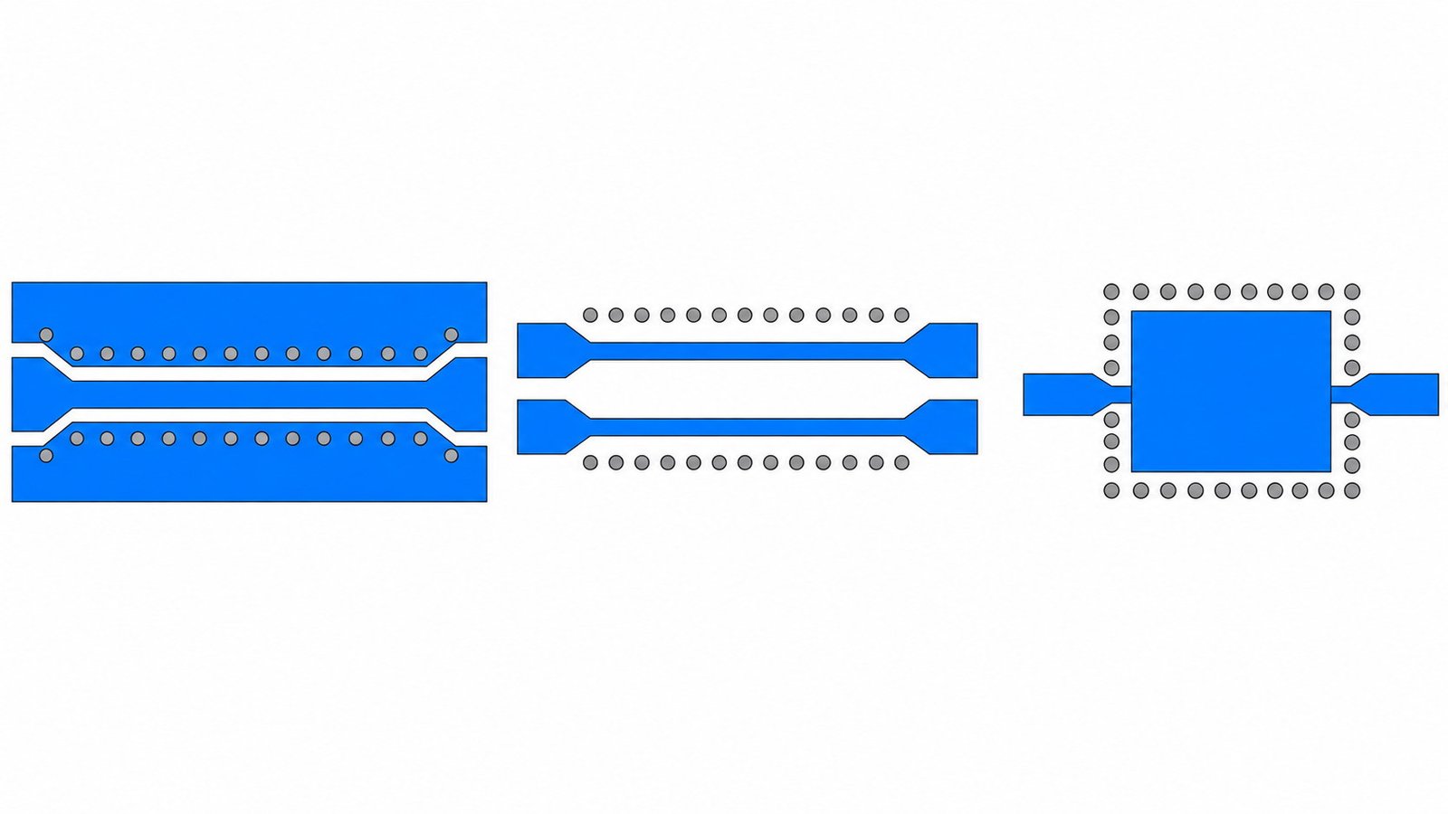
5. Layout Examples: Five Via Fence Placements
Almost every via fence on an RF board is one of five placements. They share the same spacing rule and differ in the failure mode they are guarding against — which is useful, because the failure mode tells you what to look at when a board comes back with the isolation you predicted but not the one you measured.
| Placement | Where the fence goes | Pitch | The mistake that costs the most |
|---|---|---|---|
| 1. GCPW side rails | Along both coplanar ground strips, one each side of the signal trace, tied down to the bottom ground plane. | ≤ λ/10 | Fencing one side only. A single-sided fence leaves the slotline mode in place, so the structure behaves as ungrounded CPW and the impedance is not the one the solver predicted. |
| 2. Microstrip channel isolation | Between two adjacent RF traces, or between two channels of a feed network, running the length of the parallel section. | ≤ λ/10 for full isolation; λ/8 is often adequate for 20–30 dB | Fencing the victim but not the aggressor, and stopping the fence short of the point where the two traces actually separate. |
| 3. RF block boundary | Around the perimeter of the RF section, enclosing it and separating it from digital, DC and control circuitry. | ≤ λ/10 at the highest RF frequency in the block | Leaving a wide gap where a DC feed or a control line crosses the boundary. Any crossing should be filtered at the fence line, and the gap must still respect λ/10. |
| 4. Via transition and connector launch | A ring or short arc of vias around a signal via, an edge-launch pad or a waveguide transition. | As tight as the process floor allows | Too few vias. A sparse ring does not suppress the parallel-plate mode between the two ground planes, which is exactly what the transition excites. |
| 5. Array element isolation | Between radiating elements on a patch array, and along the feed network that distributes to them. | ≤ λ/10 | Treating the fence as a substitute for element spacing. Mutual coupling is set mainly by element pitch and substrate thickness; the fence reduces surface-wave coupling, it does not remove the coupling that element spacing already allows. |
The five placements are the ones that appear in most RF layouts. They share one rule and differ only in which failure mode they are guarding against, which is why the pitch column is nearly identical across the table.
The fourth placement is the one that benefits most from a fabricator review, because a via ring around a transition competes directly with the drill floor: the tighter the ring, the more of the parallel-plate mode it suppresses. Transition geometry in detail — launch dimensions, ground return and the loss budget — is set out in our notes on SMA and 2.92 mm connector launch design, and the ground via pattern around a QFN or MMIC pad is treated in the QFN MMIC RF PCB layout guide.
6. GCPW Via Fence: A Structural Requirement
Grounded coplanar waveguide is the case where a via fence stops being an enhancement and becomes part of the transmission line itself. In GCPW the coplanar ground conductors on the top layer must be connected to the bottom ground plane through vias; if they are not, the structure behaves as ungrounded coplanar waveguide, the parasitic slotline mode is not suppressed, and the field distribution — and therefore the impedance — is not the one the design was dimensioned for.
| Requirement | Value | Reason |
|---|---|---|
| Via spacing | ≤ λ/10 at the operating frequency | Same rule as an isolation fence, but here there is no relaxed tier — the fence is part of the transmission line. |
| Sides | Both coplanar grounds | One side only leaves the parasitic slotline mode in place. |
| Pitch | Uniform along the entire line length | A local gap re-radiates and shows up as a ripple in the return loss. |
| Via-to-trace distance | Coplanar gap dimension plus the via pad clearance | Keeps the impedance the field solver predicted instead of loading the line. |
| Continuity | Same ground net as the bottom plane, reference plane unbroken | The fence is the return path for the coplanar grounds. |
Because the fence is inside the transmission line, it has to be held to the same tolerance as the line. That places it in the same design review as the impedance target itself; the coupling between controlled-impedance discipline, via fences and ground-plane integrity is covered in controlled impedance RF PCB.
7. Manufacturing Limits: Where λ/10 Meets the Drill Floor
A fence pitch requirement is only real if the process can drill it. The limits below are the ones the electrical calculation has to be checked against, and they are also the numbers that divide the frequency bands cleanly in two.
| Limit at Riching PCB | Value |
|---|---|
| Minimum mechanical drill diameter | 0.20 mm |
| Minimum via pitch, same net | 0.40 mm centre to centre (edge to edge ≥ 0.15 mm) |
| Minimum via pitch, different nets | 0.50 mm centre to centre |
| Minimum laser-drilled blind via | 0.10 mm |
| Via aspect ratio limit | 12:1, which also caps blind via depth on a thin core |
Compare the λ/10 requirement from the spacing table with the 0.40 mm same-net pitch floor and the band structure falls out:
| Band | Required λ/10 pitch (Dk 3.48) | What it means for the build |
|---|---|---|
| Up to 18 GHz | 0.89 mm or wider | Comfortable — a 0.30 mm mechanical drill at 0.8–1.0 mm pitch sits well inside both the electrical and the process limit. |
| 24–28 GHz (K / Ka band) | 0.67–0.57 mm | Standard RF work — 0.30 mm drill at 0.55–0.65 mm pitch, still above the 0.40 mm same-net floor. |
| 38 GHz | 0.42 mm | At the floor — the electrical requirement has arrived at the mechanical pitch limit. Confirm drill and pitch together during DFM. |
| 60–77 GHz | 0.27–0.21 mm | Process change required — below the mechanical pitch floor, so a laser-drilled microvia fence is the only route that meets λ/10. |
| 94–100 GHz (W band) | 0.16 mm at 100 GHz | Tightest available — laser drill at the finest achievable spacing, with the fence treated as a designed structure rather than an add-on. |
This is the table that decides whether a millimetre-wave layout is buildable as drawn. The electrical rule and the process rule are independent, and between about 35 GHz and 40 GHz they cross: below that crossing the fence is a layout decision, above it the fence becomes a process decision.
Drilling capability in more detail — hole size, aspect ratio, registration tolerance and the inspection that goes with them — is summarised in our high frequency PCB drilling capabilities page. When a fence is being pushed to the tightest pitch, it is worth verifying the result rather than assuming it: the measurement approach for millimetre-wave structures is described in mmWave PCB VNA testing.
8. Design Checklist Before Gerber Release
A via fence fails in two ways: the electrical rule is missed, or the electrical rule is met on paper and cannot be built. The checklist below catches both, and it takes less time than a re-spin.
| Check before Gerber release | Target |
|---|---|
| Highest frequency the fence has to handle | Stated explicitly on the fabrication drawing, not only in the design file |
| Fence pitch at that frequency | ≤ λ/10, or the relaxed figure with the isolation target it was chosen for |
| Drill diameter against the fence pitch | Pitch ≥ 0.40 mm for mechanical drill; laser below that |
| Fence continuity | No gap wider than λ/10 anywhere along the route, including where traces cross |
| Reference plane under the fence | Unbroken, same net as the fence vias |
| Via-to-trace clearance | Inner pad edge ≥ 1× trace width from the trace edge |
| Row count | Decided from the isolation target, not left to the layout tool default |
| DFM submission | Gerbers + NC drill + stackup + the operating frequency, so the fence can be checked against the drill floor |
One item on that list deserves a closing note. Consistency across the site matters as much as the arithmetic: a board where one fence is built at λ/10 and the next at λ/6 will pass on the bench and fail in the field, because the failure appears only when the two sections are driven together at the top of the band.
Via Fence PCB — Frequently Asked Questions
Spacing, GCPW requirements, drill and pitch limits, and when a second row is worth the area.
What is the correct via fence spacing for an RF PCB?
The maximum useful spacing between adjacent ground vias in a fence is about one tenth of the guided wavelength at the highest frequency the structure has to handle. The guided wavelength is the free-space wavelength divided by the square root of the substrate dielectric constant. On a ceramic-filled hydrocarbon laminate with a Dk of 3.48 that works out at 1.61 mm at 10 GHz, 0.67 mm at 24 GHz, 0.57 mm at 28 GHz and 0.21 mm at 77 GHz. The rule is a guideline rather than a cliff: λ/8 is often sufficient for a 20–30 dB isolation target, while the last 10 dB needed to pass 40 dB usually requires tighter-than-λ/10 pitch, or a second staggered row of vias.
Does a GCPW line need via fencing on both sides?
Yes, and on a grounded coplanar waveguide the fence is a structural element rather than an isolation enhancement. The coplanar ground conductors on the top layer have to be connected to the bottom ground plane at a spacing of λ/10 or less, on both sides of the signal trace, at a constant pitch along the whole line. Without that connection the structure behaves as ungrounded coplanar waveguide: the parasitic slotline mode is not suppressed, the field distribution is not the one that was simulated, and the characteristic impedance is therefore not the one the design was dimensioned for. Fencing a single side leaves the mode in place.
What is the minimum via fence pitch a fabricator can drill?
On a standard high-frequency process, the minimum mechanical drill diameter is 0.20 mm and the minimum via pitch on the same net is 0.40 mm centre to centre, with at least 0.15 mm of dielectric between adjacent hole edges. Vias on different nets need 0.50 mm. Laser-drilled blind vias bring that down to 0.10 mm. That is what makes the frequency bands divide: up to about 28 GHz the λ/10 requirement is comfortably above the 0.40 mm floor, at roughly 38 GHz the two figures meet, and from 60 GHz upward λ/10 is below what a mechanical drill can deliver, so a laser-drilled microvia fence is required.
Is a double row of ground vias better than a single row?
A single row typically gives 15–25 dB of isolation improvement at the design frequency, and a second staggered row adds roughly 5–10 dB on top of that. The second row is worth its area where the isolation target is above about 40 dB, on millimetre-wave designs where surface-wave suppression matters more than the extra board area, and around an RF block boundary that has to hold a sharp transition to digital circuitry. For a moderate target the single row is the better engineering choice: the second row costs routing area and adds vias to the drill file for a gain that is smaller than the gain from simply tightening the pitch of the first row.
Send us the Gerbers and the operating frequency.
We will check the via fence pitch against the drill floor for your band, confirm that the reference plane under the fence is unbroken, and tell you before you commit whether the λ/10 spacing your design needs is a mechanical or a laser-drilled route. DFM review in 4–8 hours, with the drill and pitch decision written into the quote.
Contact Us → WhatsApp: +86 137 6047 3650Request a PCB Quote
Upload your Gerber ZIP file and project requirements. Our engineering team will review your PCB material, stackup, impedance needs, surface finish, and production quantity before quoting.
Please prepare:
- Gerber files in ZIP format
- PCB material or stackup requirements
- Controlled impedance notes if available
- Prototype or batch production quantity