
Multi-Band Counter-UAS Jammer PCB: Four Bands, One Sealed Box
Counter-UAS jammer PCB design for 1.6–5.8 GHz transmitters: band-dedicated chains, sealed-shell PA dissipation, co-site isolation and the battery budget.
Home » Counter-UAS PCB » Multi-Band Counter-UAS Jammer PCB: Four Bands, One Sealed Box
Table of Contents
A wearable multi-band counter-UAS jammer is a hostile environment for its own electronics: four transmit bands into 60° apertures, a sealed shell with no convection, a control receiver that must keep working metres from its own transmitter, and a battery that everything above is charged to. The PCB sits underneath all four constraints at once.
This page is the transmitter side of the counter-UAS problem — power chains, sealed-shell thermals, co-site isolation and the energy budget. The receiving side, where the array must survive a hostile jammer, is a different board with its own discipline, covered in our GNSS anti-jamming PCB guide. All power figures below are a clearly-labelled worked example for design illustration, not any specific product's specification.
1. The Frequency Plan: Four Bands, Two Antenna Families
The bands are fixed by the threat: 2.4, 5.2 and 5.8 GHz for the drone's command and video links, 1.6 GHz for its GNSS reception. One octave and a bit of spread, four chains, one box.
| Band | λ0 in air | λ/2 patch scale | Copper skin depth |
|---|---|---|---|
| 1.6 GHz (GNSS L1) | 187 mm | 93.7 mm | 1.63 µm |
| 2.4 GHz | 125 mm | 62.5 mm | 1.33 µm |
| 5.2 GHz | 57.7 mm | 28.8 mm | 0.90 µm |
| 5.8 GHz | 51.7 mm | 25.8 mm | 0.86 µm |
A 60° coverage requirement per band pushes each antenna family toward its own aperture, and the board carries all four chains at once. The 5.8 GHz chain runs on 0.86 µm of copper skin — conductor finish quality is a real parameter at the top band.
The coverage requirement does as much architectural work as the frequency list. Sixty degrees of horizontal and vertical coverage per band, at wearable mass, pushes each band toward its own aperture — and once the apertures are separate, the transmit chains behind them usually want to be separate too. That argument is the next section.
2. Band-Dedicated Chains Beat the Shared Aperture
The tempting architecture is one wideband PA section feeding a switch-filter bank into a single multi-band antenna. The arithmetic does not survive contact with the loss table.
| Architecture element | Shared aperture + switch-filter bank | Band-dedicated chains |
|---|---|---|
| Combining / routing loss | 6.0 dB for an ideal 4-way combine — half the PA output, gone | Feed loss only, typically 0.5–1 dB per chain |
| Filter bank insertion | 0.8–1.5 dB per pass, before the PA or after it | One filter per band, in-line |
| Switching transients | Load-pull steps every band change | None — every PA sees a constant load |
| Antenna count | 1 aperture, 60° coverage is hard across 1.6–5.8 GHz | 3–4 dedicated apertures, 60° each |
| Board area | Smaller RF section, large switching section | Four parallel chains — area grows, complexity per chain drops |
The combine loss alone decides the architecture: 6 dB of combiner means the PA must supply four times the power for the same radiated level, and that power becomes heat in the sealed shell.
Six decibels of ideal combiner is not a rounding error — it is a factor of four in PA output for the same radiated level, and in a sealed shell every one of those watts becomes heat that has nowhere to convect away from. Dedicated chains cost board area and apertures; they return constant PA loads, in-line filtering per band and an architecture where each thermal problem stays local. The PA board-level rules are in our RF power amplifier PCB guide.
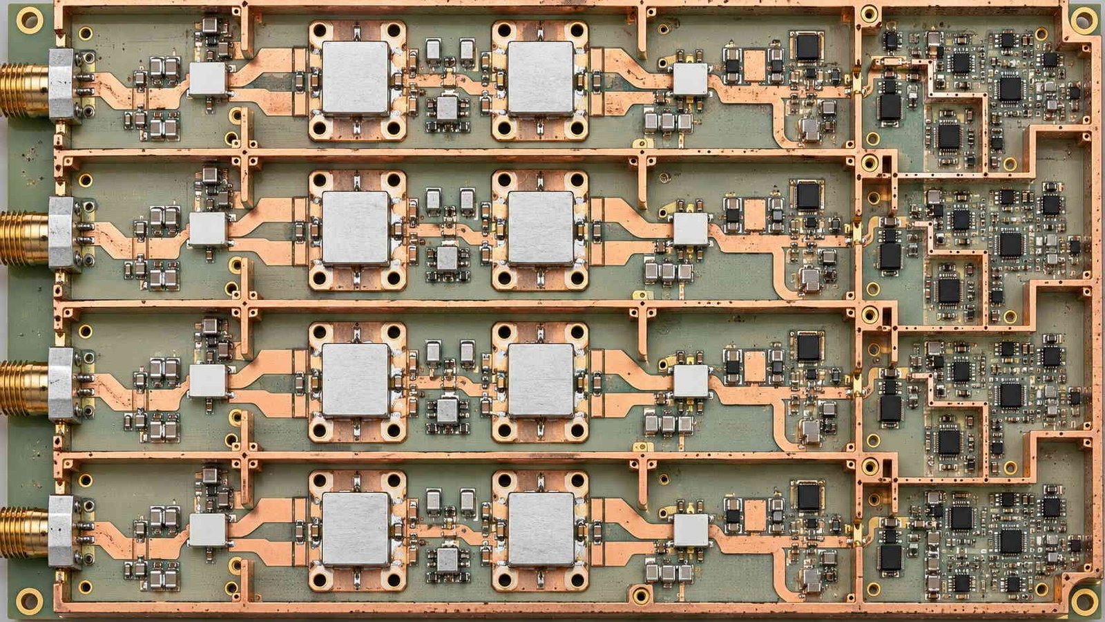
3. PA Dissipation in a Sealed Shell
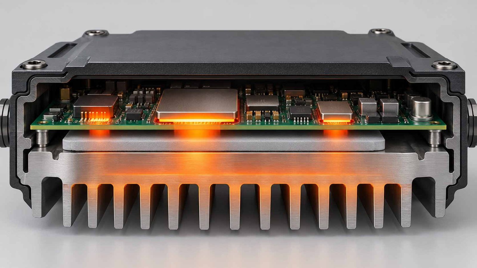
An IP67 enclosure is a thermally honest place: no vents, no fans, no convection, no excuses. Every joule the board makes must leave through conduction to the shell.
| Heat path in the sealed shell | Value at 22.3 W total heat | Comment |
|---|---|---|
| PA dissipation, 3 W RF per band at 35%% drain efficiency | 5.6 W per band | Four bands running simultaneously |
| Aluminium spreader, 3 mm over 8 cm² | 0.0 K | Negligible — not the problem |
| TIM, 0.5 mm / 1 W/mK | 1.4 K | The real design variable |
| 0.1 mm air gap under the PA | 10.7 K | Runaway — the mount is part of the spec |
An IP67 shell has no convection and no vents: every joule leaves through conduction or is stored. The PA-to-shell interface decides the junction temperature, so it gets specified — material, thickness, pressure — not assumed.
The pattern repeats from every high-power board: the spreader is not the design variable, the interfaces are. What is specific to the wearable case is that the shell itself is the heatsink, its area is fixed by ergonomics, and the PA mounting interface — TIM material, thickness, fastener pressure — becomes a specified parameter with incoming inspection, not an assembly detail. The GaN-level version of the same account is in our GaN power amplifier thermal guide.
4. Co-Site Isolation: Surviving Your Own Transmitter
The control and sensing electronics live in the same box as a legal-to-them illegal transmitter. The isolation budget between them is a system requirement, and it is written before layout, not after a bench surprise.
| Co-site isolation budget | Value | Where it comes from |
|---|---|---|
| Transmitter output | +34.8 dBm | 3 W at the PA flange (worked example) |
| Control receiver maximum input | 0 dBm | Front-end survival level |
| Required isolation | 54.8 dB | Survival plus a 20 dB margin |
| Space isolation, back-to-back 60° apertures | ≈ 45 dB | Pattern discrimination and shell shadowing |
| Cavity shielding between TX and control | ≈ 40 dB | Compartment wall, feedthrough filters |
| Structured total | ≈ 85 dB | Margin exists — but only if the compartments are real |
The budget holds only if the shielding is built as compartments, not as a wish. A single ground plane shared by an unchecked control trace and a PA return is how 85 dB of structure becomes 40 dB of reality.
Two details decide whether the structured budget survives contact with manufacturing. The compartment wall has to be a compartment — a single unbroken ground shared by a PA return and an unchecked control trace converts 85 dB of structure into 40 dB of reality. And every signal crossing the wall goes through a feedthrough filter, because a wire through a hole in the shield is a wire around the budget. Receiver-side grounding and shielding discipline is in our LNA grounding and shielding guide.
5. The Battery and Mass Account
On a wearable, electrical efficiency is a logistics decision. Every watt the PA wastes or the control section leaks is carried on the operator's back for the whole mission.
| Wearable account | Value | Note |
|---|---|---|
| Total DC draw, four bands plus overhead | 42.3 W | PA 34.3 W, switching/control/power conversion 8 W |
| Energy for 2 hours of continuous operation | 85 Wh | Set by the mission profile, not the battery catalogue |
| Cells required | 7 × 18650 (86 Wh) | 0.34 kg of battery alone |
| Cost of every watt saved at the PA | ≈ 7.8 g of battery | Efficiency and duty management pay in grams |
The wearable constraint inverts the usual priorities: the PA efficiency term and the control-section overhead are not electrical details, they are the mass budget.
Seven grams per watt does not sound like much until it is multiplied by a duty cycle, a mission profile and an operator. It is why the efficiency term in the PA selection and the overhead term in the power tree belong in the RFQ — they are mass budget lines that happen to be measured in watts. The mixed-signal discipline that keeps the control section lean is in our RF and digital mixed-signal stackup guide.
6. The Counter-UAS Board RFQ Checklist
Related reading
- digital beamforming satellite array PCB — Ka-band element pitch, mixed-signal stack-up and batch phase consistency
- GNSS anti-jamming PCB — CRPA arrays and multi-RF isolation on the receive side
- RF power amplifier PCB design — matching, stability and thermal path
- GaN PA thermal design — heat spreading from a small die
- aerospace and defence high-frequency PCB — qualification and traceability for mission hardware
Eight lines, and the first conversation should be about the last one.
| # | Item to specify | Why it decides the outcome |
|---|---|---|
| 1 | Band list and per-band RF power | Sets the chain count, the thermal account and the battery |
| 2 | Coverage pattern per band (60° cones) | Aperture choice per band; shared-aperture loss is avoided by design |
| 3 | Architecture: dedicated chains confirmed | A 6 dB combiner silently quadruples the PA and the heat |
| 4 | PA-to-shell interface specification | TIM material, thickness, fastener pressure — the junction temperature |
| 5 | Co-site isolation budget with margin | 85 dB structured vs the 54.8 dB the receiver needs |
| 6 | Control-section shielding and feedthrough filtering | Keeps the digital truth out of the transmit chains |
| 7 | Duty cycle and thermal soak data | 2 h continuous is a different board from 10%% duty |
| 8 | End-use and export documentation up front | Controlled goods: the compliance review leads the RFQ, not trails it |
Eight lines. Lines 3, 4 and 8 are the three that most often arrive too late.
The pattern: a counter-UAS transmit board is specified by its losses and its interfaces — combining loss avoided by architecture, thermal resistance specified at the mount, isolation budgeted with margin and verified on the first article. The compliance review leads the RFQ because every technical line after it depends on the programme being real.
Multi-Band Counter-UAS Jammer PCB — Frequently Asked Questions
Band-dedicated transmit chains, sealed-shell PA dissipation, co-site isolation budgets, the battery account and where the compliance review belongs.
Why four separate transmit chains instead of one wideband PA and a switch?
Because the losses stack against you. A 4-way combine costs 6.0 dB even in its ideal form — the PA must deliver four times the power for the same radiated level, and every added watt becomes heat inside a sealed shell with no convection. Band-dedicated chains pay with board area and three extra apertures, and get back constant PA loads, in-line filtering and a thermal account that closes. At 1.6–5.8 GHz the apertures are small enough that four of them fit where a broadband 60° design would struggle anyway.
How do you keep the jammer from jamming itself?
Compartmentalisation, quantified. In the worked example the transmitter is +34.8 dBm and the control receiver needs its input held below 0 dBm with a 20 dB margin — about 55 dB of isolation. Roughly 45 dB comes from space: back-to-back 60° apertures and the shadow of the shell. Another 40 dB comes from a real compartment wall with feedthrough filters. The number only holds if the wall exists as drawn, which is why the isolation budget is verified on the first article, not on the datasheet.
Where does the heat go in a sealed IP67 enclosure?
Through the interfaces, by conduction only. Four bands at 3 W RF and 35% drain efficiency dissipate about 22.3 W. A 3 mm aluminium spreader contributes 0.0 K; a half-millimetre TIM contributes 1.4 K; an unintentional 0.1 mm air gap under the PA contributes 10.7 K and a thermal shutdown. The PA mounting interface is therefore specified like an electrical parameter — material, thickness and pressure — because that is exactly what it is.
Does a transmit jammer board have anything to do with GNSS anti-jamming design?
They are two ends of the same problem and the board disciplines overlap more than the labels suggest. Anti-jamming work — CRPA reception, multi-RF isolation, proof against a hostile transmitter — is covered in our GNSS anti-jamming PCB guide. This page is the transmitter side: power amplifiers, band filtering, sealed-shell thermals and co-site isolation. A programme usually needs both boards to coexist in one system, and the isolation budget between them is a system-level requirement that has to be written down once, not discovered twice.
What actually drives the battery size?
The DC draw, which is dominated by the PAs and their efficiency. In the worked example, four bands at 3 W RF and 35% efficiency draw 34.3 W, plus about 8 W for switching, control and power conversion — 42.3 W for two hours is 85 Wh, or 7 cells at 0.34 kg. The leverage runs the other way too: every watt trimmed from PA inefficiency or control overhead is roughly 7.8 g of battery that does not have to be carried.
What should an RFQ for this class of board lead with?
The compliance statement, before the stackup. Counter-UAS transmit hardware is controlled goods in most jurisdictions, and a manufacturer who takes the end-use and export review seriously will ask for it first — treating it as paperwork at the end of the RFQ is how programmes lose months. After that: the band list and per-band power, the coverage requirement, the duty cycle, the thermal environment and the isolation budget. Our aerospace and defense PCB page describes the qualification and traceability framework behind such programmes.
Building a multi-band transmit board for a counter-UAS programme?
Send the band list and per-band power, the coverage requirement, the duty cycle and the thermal environment. We will architect the chains to keep the PA load constant, size the PA-to-shell interface, close the co-site isolation budget with margin, and return a stackup with the thermal and isolation accounts — plus the compliance documentation package — alongside the quote.
Contact Us → WhatsApp: +86 137 6047 3650Request a PCB Quote
Upload your Gerber ZIP file and project requirements. Our engineering team will review your PCB material, stackup, impedance needs, surface finish, and production quantity before quoting.
Please prepare:
- Gerber files in ZIP format
- PCB material or stackup requirements
- Controlled impedance notes if available
- Prototype or batch production quantity