Copper thickness is one of the most important parameters in RF and microwave PCB design, but it is often confirmed too late in the project review process. The copper weight on each layer — measured in ounces per square foot — directly determines the minimum line width and line spacing that can be reliably produced. It also affects etching tolerance, impedance calculation, and the final electrical performance of RF traces.
For RF PCB, microwave PCB, Rogers PCB, PTFE PCB, and antenna PCB, selecting the right copper weight at the design stage prevents manufacturing problems, impedance deviation, and prototype failures.
This guide explains how copper thickness affects line width minimums, etching behavior, and manufacturing tolerances, and what to confirm before sending RF PCB files for production.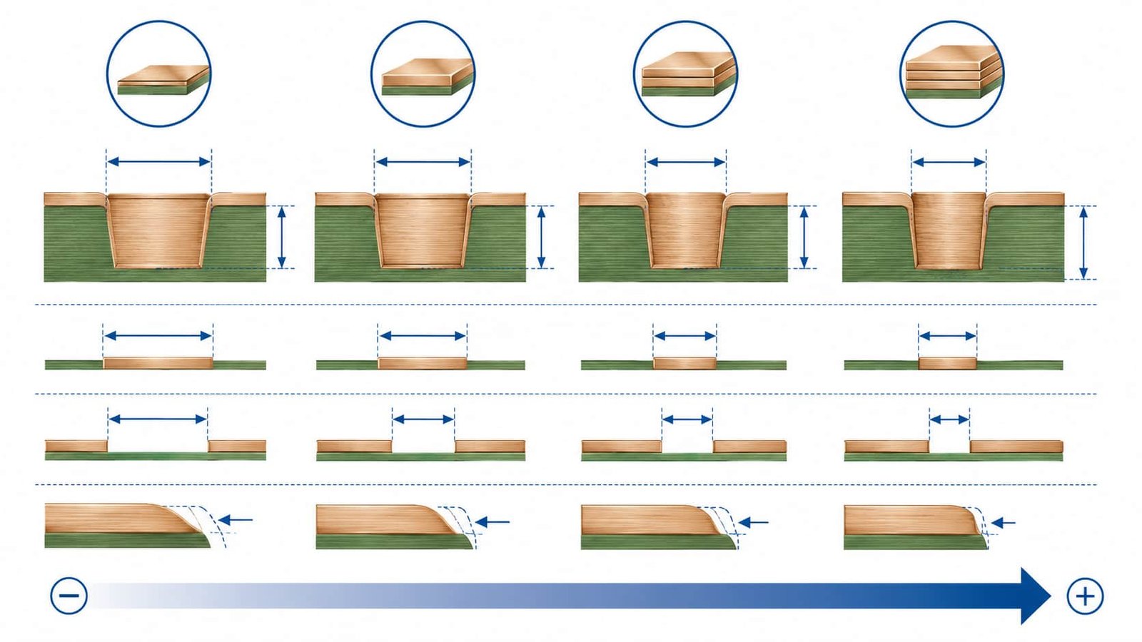
Quick Summary
Key point: Thicker copper requires wider minimum line widths and larger minimum line spacing. For RF and microwave PCB, copper weight on signal layers is typically 0.5 oz to 2 oz. Heavy copper (3 oz and above) is used for power or thermal layers, not fine RF traces. Confirm copper weight and minimum line width together during stackup review.
Copper weight ranges from 0.5 oz to 5 oz for standard production, with inner layers up to 12 oz and outer finished layers up to 13 oz in advanced capability. Each step up in copper weight increases the minimum producible line width and affects etching tolerance, which directly impacts controlled impedance consistency.
What Copper Weight Means in PCB Manufacturing
Copper weight in PCB manufacturing refers to the weight of copper per square foot of board surface, measured in ounces. It is a conventional way of specifying copper layer thickness.
- 5 oz copper = approximately 17.5 µm thick
- 1 oz copper = approximately 35 µm thick
- 2 oz copper = approximately 70 µm thick
- 3 oz copper = approximately 105 µm thick
- 4 oz copper = approximately 140 µm thick
For outer layers, the final finished copper thickness is higher than the starting foil weight because copper is added during the plating process. For inner layers, the copper thickness is closer to the original foil weight since inner layers are not plated after lamination.
Important: When specifying copper weight for an RF PCB stackup, always clarify whether you mean starting foil weight or finished copper thickness. The difference matters for impedance calculation and line width minimums.
Why Copper Thickness Matters for RF and Microwave PCB
In RF and microwave circuit design, trace geometry directly determines electrical performance. Line width controls characteristic impedance. Line spacing controls coupling, crosstalk, and isolation between adjacent RF signals. Both are affected by copper weight.
Effect on Minimum Line Width
Thicker copper is harder to etch cleanly. The etching process removes copper laterally as well as vertically, creating a trapezoidal trace cross-section known as the etch factor. Thicker copper means more lateral etching is needed to clear the spaces between traces, which increases the minimum line width that can be reliably produced.
Effect on Impedance
Controlled impedance calculation must account for the actual copper thickness, not just the dielectric thickness and trace width. A thicker copper trace has a slightly different impedance than a thin copper trace of the same nominal width. If copper weight changes from the specified value, the final impedance may shift outside tolerance.
For impedance control background, see Why Controlled Impedance Matters in RF PCB Manufacturing.
Effect on Skin Depth at High Frequencies
At RF and microwave frequencies, current flows primarily in a thin layer at the surface of the conductor — the skin depth. For most RF applications above 1 GHz, the skin depth is well below 1 oz copper thickness. This means increasing copper thickness beyond a certain point does not reduce RF loss further, but it does increase the minimum line width requirement and material weight.
Inner Layer Minimum Line Width by Copper Weight
The table below shows minimum line width and line spacing requirements for inner layers at different copper weights. Inner layers are not plated, so the copper weight is closer to the original foil specification.
Copper Weight | Min. Line Width (Standard) | Min. Line Width (Advanced) | Min. Line Space (Standard) |
1/3 oz | ≥ 6.5 mil | ≥ 5.5 mil | ≥ 6.5 mil |
H oz (0.5 oz) | ≥ 7 mil | ≥ 6 mil | ≥ 7 mil |
1 oz | ≥ 8 mil | ≥ 7 mil | ≥ 8 mil |
2 oz | ≥ 9 mil | ≥ 8 mil | ≥ 9 mil |
3 oz | ≥ 12 mil | ≥ 11 mil | ≥ 12 mil |
4 oz | ≥ 15 mil | ≥ 14 mil | ≥ 15 mil |
5 oz | ≥ 18 mil | ≥ 17 mil | ≥ 18 mil |
6 oz | ≥ 19 mil * | ≥ 18 mil * | ≥ 19 mil * |
* 6 oz copper: double-sided etching process required. Engineering review needed.
Design guidance: For RF signal layers on inner layers, 1 oz copper is the most common choice. It offers a good balance between line width minimums, etching consistency, and impedance control. Half oz (0.5 oz) is used when very fine lines are required. 2 oz and above are typically reserved for power or ground planes, not fine RF traces.
Outer Layer Minimum Line Width by Copper Weight
Outer layer copper weight includes the starting foil plus plating added during the electroplating process. The finished outer layer copper is typically heavier than the inner layer copper. This must be accounted for in impedance calculations and line width minimums.
Copper Weight | Min. Line Width (Standard) | Min. Line Width (Advanced) | Min. Line Space (Standard) |
1/3 oz | ≥ 5 mil | ≥ 3.5 mil | ≥ 4 mil |
H oz (0.5 oz) | ≥ 5 mil | ≥ 4 mil | ≥ 4 mil |
1 oz | ≥ 6 mil | ≥ 4.5 mil | ≥ 5 mil |
1.5 oz | ≥ 6.5 mil | ≥ 6 mil | ≥ 5.5 mil |
2 oz | ≥ 7 mil | ≥ 6.5 mil | ≥ 6 mil |
3 oz | ≥ 9 mil | ≥ 8 mil | ≥ 8 mil |
4 oz | ≥ 12 mil | ≥ 11 mil | ≥ 10 mil |
5 oz | ≥ 15 mil | ≥ 13 mil | ≥ 12 mil |
6 oz | ≥ 20 mil * | ≥ 18 mil * | ≥ 18 mil * |
* 6 oz copper: double-sided etching process required. Engineering review needed.
Note: Outer layer finished copper weight is the result of starting foil plus plating. For standard 1 oz outer layers, the finished copper is typically 1.2–1.5 oz after plating. This means the impedance must be calculated using the finished copper thickness, not the starting foil weight. Confirm with your manufacturer which value to use in your impedance stack calculation.
Etching Tolerance and Its Effect on RF Trace Accuracy
Etching tolerance refers to how closely the finished trace width matches the design target after the chemical etching process. For RF PCB, trace width accuracy is critical because even small deviations from the design width can shift the characteristic impedance outside the acceptable range.
Standard Etching Tolerance
- Line width and spacing < 10 mil: tolerance ±1 mil
- Line width and spacing ≥ 10 mil: tolerance ±20%
Impedance Trace Etching Tolerance
- Line width and spacing < 10 mil: tolerance ±1 mil
- Line width and spacing ≥ 10 mil: tolerance ±10%
For controlled impedance traces, the tighter ±10% tolerance applies to traces at or above 10 mil width. Fine traces below 10 mil are held to ±1 mil absolute tolerance regardless of impedance requirement.
How Etching Tolerance Affects Impedance
A 1 mil change in trace width can shift impedance by 2–5 ohms depending on the dielectric thickness and Dk value. For a 50-ohm microstrip line on a thin Rogers substrate, even a 0.5 mil width deviation may push the impedance outside ±10% tolerance.
This is why copper weight, trace width, and etching tolerance must be confirmed together during the pre-production stackup review, not treated as independent parameters.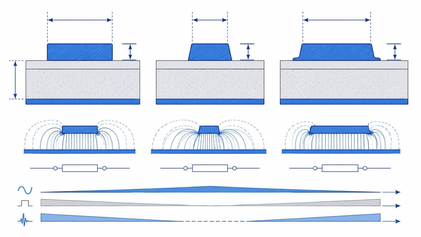
Selecting Copper Weight for RF Signal Layers
The right copper weight for an RF signal layer depends on the minimum trace width in the design, the impedance target, the frequency range, and the application.
0.5 oz (H oz) Copper — Fine RF Traces
Used when the design requires very fine line widths, typically below 5 mil on outer layers. Common in compact RF modules, millimeter-wave circuits, and high-density antenna PCB where space is limited and fine pitch is needed. Provides the tightest line width minimums but requires careful handling and inspection.
1 oz Copper — Standard RF Signal Layer
The most common copper weight for RF and microwave PCB signal layers. Supports minimum outer layer line widths from 4.5–6 mil depending on process. Good balance between line width capability, etching consistency, and impedance control. Used in most Rogers PCB, PTFE PCB, and Taconic high frequency board designs.
2 oz Copper — RF Power and Ground
Used for RF power amplifier input and output traces, heavy current paths, or ground planes that also carry thermal load. Minimum line width increases to 6.5–7 mil on outer layers. Not typically used for fine impedance-controlled signal traces.
3 oz to 6 oz Copper — Heavy Copper Applications
Used for power stages, thermal management layers, RF power amplifier boards, and high-current RF connectors. Not suitable for fine RF signal traces. Minimum line widths start at 9 mil and increase with copper weight. Double-sided etching process required for 6 oz and above.
For heavy copper in RF power amplifier boards, see RF Power Amplifier PCB: Material, Stackup and Thermal Review.
Copper Thickness in Impedance Stackup Calculation
When planning a controlled impedance stackup for RF or microwave PCB, copper thickness must be included in the calculation alongside dielectric constant, dielectric thickness, and trace geometry.
- Inner layer copper weight affects dielectric thickness after lamination — thicker copper compresses the prepreg more
- Outer layer finished copper weight must use the plated thickness, not starting foil
- Different copper weights on signal vs reference planes change the effective dielectric thickness
- Impedance software and field solvers require actual copper thickness, not nominal foil weight
- After production, impedance coupons are used to verify that the finished board meets the target impedance within tolerance
For stackup planning and impedance review, see RF PCB Stackup Design: Key Factors Before Manufacturing.
Copper Thickness Considerations for Rogers and PTFE PCB
Rogers and PTFE high frequency materials have specific copper foil options that affect both RF performance and minimum line width capability.
Rolled Annealed (RA) Copper vs Electrodeposited (ED) Copper
Rogers and PTFE laminates may be supplied with either rolled annealed (RA) copper or electrodeposited (ED) copper foil. RA copper has a smoother surface, which reduces copper surface roughness and lowers insertion loss at microwave frequencies. ED copper is more common and lower cost, but has higher surface roughness.
- RA copper: lower insertion loss at high frequency, preferred for millimeter-wave and low-loss designs
- ED copper: standard for most RF PCB applications, adequate up to Ka-band for most designs
- Some Rogers materials such as RO4350B are available with LoPro copper foil for reduced roughness
For Rogers material selection and properties, see Rogers PCB Material Selection Guide for RF and Microwave Applications.
Copper Thickness Information Needed for RF PCB Quotation
To review copper weight feasibility and provide an accurate quotation, the following information should be included with the design files:
- Gerber files with trace geometry clearly defined
- Complete PCB stackup specifying copper weight on each layer
- Whether outer layer copper weight is starting foil or finished plated thickness
- Minimum line width and line spacing in the design
- Controlled impedance requirements with target values and tolerance
- Material type — Rogers, PTFE, Taconic, F4B, or FR4 hybrid
- Surface finish — ENIG, immersion silver, OSP, or other
- Layer count and board thickness
- Quantity — prototype or batch
- Working frequency or application background
For a complete quotation checklist, see What Files Are Needed for a High Frequency PCB Quotation?.
Conclusion
Copper thickness is a fundamental parameter in RF PCB manufacturing that affects minimum line width, etching tolerance, impedance calculation, and final board performance. Thicker copper requires wider traces, larger spacing, and tighter process control to maintain impedance consistency.
For most high frequency PCB signal layers, 0.5 oz to 1 oz copper provides the best balance between fine line capability and etching reliability. Heavy copper from 2 oz and above is reserved for power, ground, and thermal layers. Confirming copper weight, line width minimums, and etching tolerance during the pre-production stackup review reduces impedance deviation risk and improves prototype and batch consistency.