
Cryogenic RF PCB: Contraction, Heat Load and 4 K Signal Integrity
Cryogenic RF PCB guide: 300 K to 4 K thermal contraction, cold-stage heat budget, copper trace heat leak and dielectric stability for quantum systems.
Table of Contents
Cryogenic RF used to be a laboratory one-off: a physicist, a copper plate, and a board that had been made by whoever would answer the phone. That is changing. High-density cryogenic RF connector ranges — multiple low-temperature channels in one shell, filters and attenuators integrated into the cable assembly — are now catalog products, and sealed IP-rated interconnect families are being shown alongside them. When the interconnect becomes a product, the board behind it becomes a specification.
This page computes four things that decide whether such a board works: how much the laminate and the plated barrels disagree about shrinking between 300 K and 4 K; what the attenuation chain actually dissipates on each cooling stage; how much heat a copper trace carries between stages; and how far a dielectric drift moves a filter. Then it maps the fabrication records that stand in for inspection, because a cryostat gives you exactly one chance to be right.
The room-temperature topics are covered elsewhere: impedance method in our controlled impedance PCB guide, cold measurement in the mmWave PCB VNA testing guide. This page is about the part of the temperature range that ordinary qualification never visits.
1. A Board That Changes Size by One Percent
Everything in a cryostat shrinks. The problem is that the parts do not shrink by the same amount.
| Material in the stack | Integrated contraction 300 K → 4 K | Mismatch vs copper | Displacement over 1.6 mm / 2.4 mm |
|---|---|---|---|
| PTFE-glass laminate | 1.40% | +1.07% | 17.1 µm / 25.7 µm |
| Hydrocarbon ceramic laminate | 0.25% | −0.08% | 1.3 µm / 1.9 µm |
| FR-4 (in-plane) | 0.30% | −0.03% | 0.5 µm / 0.7 µm |
| Copper (plated barrel) | 0.33% | reference | — |
| Aluminium 6061 cold plate | 0.41% | +0.08% | 1.3 µm / 1.9 µm |
| Stainless 304 (coax) | 0.29% | −0.04% | 0.6 µm / 1.0 µm |
| Invar / kovar frame | 0.03% | −0.30% | 4.8 µm / 7.2 µm |
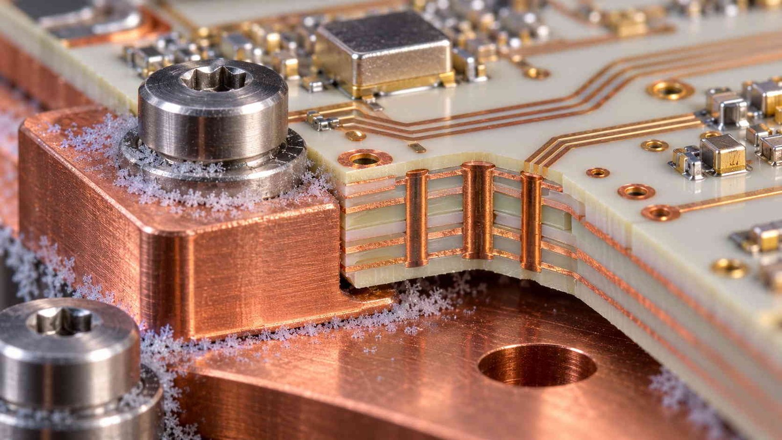
Integrated contraction values are industry-typical figures for the material classes, not specifications of any supplier’s product (stated assumption). The arithmetic that matters is the mismatch column: copper’s elastic strain limit is roughly 0.2–0.3%, so a 1.07% differential means the plated barrel has to absorb 17 µm over a 1.6 mm board — by yielding. That is why the first cooldown, not the first power-up, is the event that finds the weak barrels.
The failure this arithmetic predicts is specific: the plated barrel, which is copper, is restrained by a laminate that wants to contract three to four times as much. Copper yields at roughly 0.2–0.3% strain; the differential here is 1.07%. So the barrel deforms plastically on the first cooldown, and whether it survives is a question of wall thickness, aspect ratio and how the pads anchor it — not of plating quality alone.
2. Specifying by the Axis That Matters
No material wins every column. The specification question is which column the design leans on.
| Material class | Contraction | The axis it optimises | Where your design leans on it |
|---|---|---|---|
| PTFE-glass | 1.40% | Dk stability and loss at 4 K | Low-loss cryo front ends — barrel and pad design must absorb the 1.07% differential (section 1) |
| Hydrocarbon ceramic | 0.25% | Contraction match to copper | Large boards, many vias, cold-plate mounted assemblies where strain dominates |
| FR-4 | 0.30% | Cost and mechanical familiarity | Digital/DC and control layers where RF loss is not the binding constraint |
| Aluminium 6061 | 0.41% | Thermal conduction and machinability | Cold plates — the plate, not the laminate, usually sets the clamping strain |
Each class optimises one axis and pays for it on another; the job at specification time is to say which axis the design depends on. Contraction and dielectric behaviour both land on the same drawing, which is why the cryogenic decision is a stackup decision. Material families are set out in our high-frequency PCB materials review, the PTFE class in PTFE materials, and the comparison arithmetic in the PCB material comparison chart.
The trap in cryogenic procurement is buying one property and inheriting another. A laminate chosen for its dielectric behaviour arrives with a contraction figure attached, and both end up on the same drawing — which is why the cryo decision is a stackup review, not a materials order. The material families are set out in our high-frequency PCB materials review, the PTFE class in PTFE materials, and the selection arithmetic in the PCB material comparison chart.
3. The Heat Budget Is a Board Decision
A dilution refrigerator is a chain of cooling stages, and each stage has a power budget that sounds like a rounding error until something dissipates into it.
| Stage (0 dBm into the line) | Attenuation there | Power in | Power out | Dissipated at that stage | Against its cooling budget |
|---|---|---|---|---|---|
| 4 K stage | 20 dB | 1000 µW | 10.0 µW | 990 µW | 0.07% of a 1.5 W budget — irrelevant |
| Still (~0.7 K) | 0 dB | 10.0 µW | 10.0 µW | 0 | — |
| Mixing chamber (~10 mK) | 10 dB | 10.0 µW | 1.0 µW | 9.0 µW | 90% of a 10 µW budget — the whole margin |
| Mixing chamber, if the 10 dB sits upstream | 20 dB | 100 µW | 1.0 µW | 99 µW | 10× over budget — the stage never reaches base |
Attenuation pads are components on the board, so the staging decision is a board decision. The total attenuation is not the number that matters — the distribution is. A 4 K stage can swallow a milliwatt without noticing; the mixing chamber cannot swallow ten microwatts of anything, which is why the last pad before the sample is specified by the power that arrives at it, not by the isolation the link wants. 1.5 W at 4 K and 10 µW at the mixing chamber are representative dilution-refrigerator figures (stated assumption).
The lesson is that attenuation placement is not a link-budget detail — it is a thermal decision made on the board, because the pads sit on the board. A 4 K plate can absorb a milliwatt and never notice; the mixing chamber has ten microwatts to give, and a single 10 dB pad consumes nine of them. Moving that pad one stage up the chain changes the refrigerator’s base temperature more than any change of connector.
4. Copper Is a Heat Pipe Between Stages
The same copper that makes a good conductor at 4 K makes an excellent thermal short.
| Thermal path between two stages (100 mm) | Conductance | Heat leak over 3.99 K | Versus a 10 µW mixing-chamber budget |
|---|---|---|---|
| 0.6 mm × 35 µm copper trace on the board | 63 µW/K | 251 µW | 25× over |
| 1.6 mm × 10 mm laminate section | 8.0 µW/K | 32 µW | 3.2× over |
| 1.6 mm × 2 mm laminate section | 1.6 µW/K | 6.4 µW | 0.6× — inside budget |
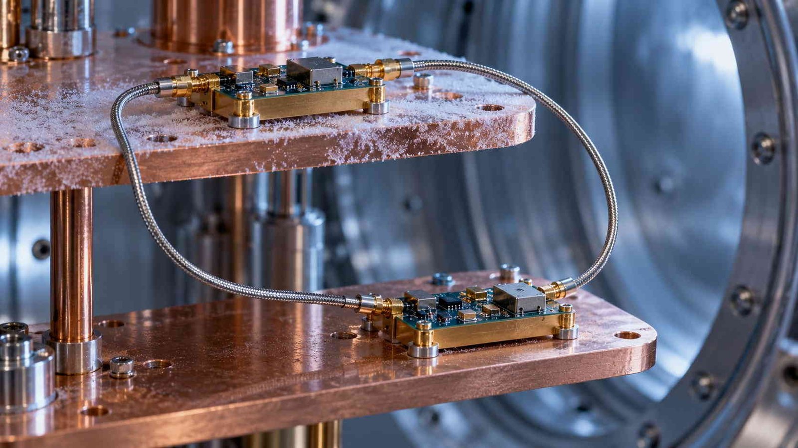
Copper at 4 K carries heat like a wire carries current — k ≈ 300 W/mK for RRR~50 material is an order of magnitude above its room-temperature value. A single 50 Ω microstrip running from the 4 K plate to the mixing chamber therefore dumps 251 µW into a stage that can only remove 10 µW. The design consequence is architectural: split the RF chain into per-stage boards, join them with stainless coax, and narrow every laminate bridge that has to cross a temperature boundary. Conductivities and stage budgets are stated assumptions.
This is why cryogenic wiring is architecturally segmented: one board per temperature stage, stainless coax between them, and laminate bridges narrowed wherever a signal has to cross a boundary. A single continuous microstrip from the 4 K plate to the sample is not an integration convenience — it is a 251 µW heater aimed at a stage that can remove 10 µW. The narrow-bridge row shows the cheap version of the fix: five times less copper width, five times less leak, without changing material.
5. Dk at 4 K: Stable Dielectric, Moving Filters
The dielectric story is quieter than the mechanical one, and easier to miss until a filter measures off-frequency.
| Dielectric class (assumed drift) | Resonance shift | At 6 GHz | Against a 60 MHz (1%) filter bandwidth |
|---|---|---|---|
| PTFE class, Dk −1% | +0.50% | +30 MHz | Half the bandwidth — retune or accept margin loss |
| Ceramic-filled hydrocarbon, Dk −3% | +1.53% | +92 MHz | 1.5× the bandwidth — the filter no longer sits where it was designed |
Resonance scales as 1/√Dk, so a 1% dielectric change moves a filter by 0.5% — 30 MHz at 6 GHz, against a 60 MHz bandwidth. The drift classes above are illustrative assumptions, not measured values: the point is that the number is the same order as the bandwidth, so room-temperature S-parameters cannot be extrapolated to 4 K. Verification at temperature — coupons measured cold, or de-embedded through the cryostat cabling — is the only honest answer, and the method is set out in our mmWave PCB VNA testing guide.
Because resonance scales as 1/√Dk, half a percent of dielectric change is half a percent of frequency — and narrowband filters do not have half a percent to spare. The drift classes above are illustrative, not measured: the point is that the shift is the same order as the bandwidth, so a room-temperature sweep proves nothing about 4 K behaviour. Cold measurement or de-embedding through the cryostat cabling is the only honest answer; the method is treated in our mmWave PCB VNA testing guide.
6. Buried, Cold and Uninspectable: What Evidence Replaces Inspection
A cryogenic assembly is inspected exactly never. It is plated, sealed, mounted and cooled, and after that nobody looks at it again.
| Fabrication record | What it proves at 4 K | Why it cannot be checked afterwards |
|---|---|---|
| Laminate batch contraction data | The stackup CTE assumption behind every via | The via is already plated; the material’s history is the only evidence |
| Thermal cycling 300 K ↔ 4 K, with PTH microsection | Barrel integrity after the strain the math predicts | A cracked barrel may still pass at room temperature |
| Coupon S-parameters measured cold (or de-embedded) | Filter and line behaviour at operating temperature | A 30 MHz shift is invisible on a 300 K measurement |
| Non-magnetic finish statement | No nickel-bearing finish in the signal path | Magnetic response is a system-level property discovered late |
| ASTM E595 outgassing data (TML / CVCM) | Vacuum compatibility inside the cryostat | Condensation on cold surfaces is a contamination event, not a rework |
| Ionic cleanliness and residue records | Surface chemistry the sample can live with | Residues are not visible in a finished assembly |
A cryostat is a place where inspection is impossible: the board is sealed, cold and mounted before anyone can look at it. Acceptance therefore rests on records produced before assembly, plus first-article cold measurement. Wide-temperature behaviour of laminates is treated in our wide-temperature PCB guide, and the probe/de-embedding mechanics in the RF and mmWave test fixture PCB design guide.
Read the table as a procurement list: every row is something to ask for before the boards are built, because after cooldown the only available evidence is what was recorded earlier. Wide-temperature laminate behaviour is treated in our wide-temperature PCB guide, and the probe and de-embedding mechanics in the RF and mmWave test fixture PCB design guide.
7. The Cryogenic RFQ Checklist
Eight lines, each traceable to a number computed above or a mechanism that cannot be inspected later.
| # | Drawing or PO line item | Why it is on the list |
|---|---|---|
| 1 | Operating stages and their cooling budgets (4 K, still, mixing chamber) | The last attenuator pad is specified by the power arriving there (section 3) |
| 2 | Board split by temperature stage, with the interconnect between stages named | A single continuous microstrip dumps 251 µW into a 10 µW stage (section 4) |
| 3 | Laminate class with its contraction figure, and the barrel design that absorbs the mismatch | 1.07% differential yields the plated barrel on first cooldown (section 1) |
| 4 | Cold-plate material and clamping method, with flatness and mounting-hole tolerance | The plate, not the laminate, often sets the strain (section 2) |
| 5 | Non-magnetic finish specified by name, not by "ENIG equivalent" | Nickel-bearing finishes are the default and the wrong default here (section 6) |
| 6 | Outgassing requirement (ASTM E595 limits) on laminate, mask and finish | Contamination inside a cryostat is not reworkable (section 6) |
| 7 | Thermal cycling regime (300 K ↔ 4 K, cycles) with PTH microsection on first article | The failure mode is invisible at room temperature (section 6) |
| 8 | Cold coupon measurement or de-embedding plan, with the reference plane defined | A 0.5% shift is the same order as the filter bandwidth (section 5) |
Eight lines. Items 1–4 decide whether the assembly survives cooldown; 5–8 decide whether anyone can prove it afterwards. A cryogenic RFQ carrying these eight answers is quotable on engineering rather than on price alone.
The pattern: cryogenic boards are specified by the failure modes that appear after cooldown, and paid for by the records that predict them. For the low-noise chains that sit at the cold end of such a system, our low-noise amplifier PCB design guide covers the grounding and shielding side.
Cryogenic RF PCB — Frequently Asked Questions
Contraction and barrel failure, stage-by-stage heat budgets, why one board cannot span the chain, dielectric drift at 4 K, and the RFQ list.
What makes a PCB cryogenic rather than just cold-rated?
The temperature is only part of it. A cryogenic board operates where the materials change dimension, conductivity and dielectric behaviour at once: from 300 K to 4 K a PTFE-glass laminate contracts about 1.4% while its plated copper barrels contract about 0.33%, so the barrel must absorb roughly 17 µm over a 1.6 mm board by yielding. Add vacuum outgassing limits, non-magnetic finish requirements and microwatt-level heat budgets, and the design problem is different in kind, not degree.
Why does the plated through hole fail on the first cooldown?
Because the laminate contracts about three to four times more than the copper that fills it. Copper's elastic strain limit is around 0.2–0.3%; the differential here is about 1.07%, so the barrel cannot stay elastic. It yields, and in the wrong geometry — thin walls, large aspect ratio, rigid pads — it cracks. The crack is often invisible at room temperature because the copper is pushed back into contact when the board warms. That is why cycling plus microsection, not a room-temperature continuity test, is the acceptance method.
How is the heat budget calculated for the RF chain?
Stage by stage. With 0 dBm into the line, 20 dB of attenuation at the 4 K stage leaves 10 µW heading down; a 10 dB pad at the mixing chamber then dissipates 9 µW of it — 90% of a typical 10 µW cooling budget. Move that 20 dB pad to the mixing chamber instead and it dissipates 99 µW, ten times the budget. The total attenuation is identical in both cases; the distribution is what decides whether the refrigerator reaches base temperature.
Can one board carry the RF from room temperature to the mixing chamber?
Not usefully. Copper at 4 K conducts heat far better than at room temperature — a single 0.6 mm × 35 µm trace over 100 mm gives about 63 µW/K, or 251 µW across the 4 K to 10 mK span, against a 10 µW budget. The laminate alone contributes about 32 µW. Practical cryostats therefore split the RF chain into per-stage boards joined by stainless coaxial lines, and narrow any laminate bridge that has to cross a temperature boundary.
What should a cryogenic RFQ include?
The operating stages and their cooling budgets, the board split by stage with the interconnect named, the laminate class with its contraction figure and the barrel design that absorbs the mismatch, the cold-plate material and clamping method, the non-magnetic finish specified by name, ASTM E595 outgassing limits, the thermal cycling regime with first-article microsection, and the cold-measurement or de-embedding plan with a defined reference plane.
Building a board that has to work at 4 K?
Send the temperature stages and their cooling budgets, the board split, the laminate contraction figure and your cold-plate arrangement. We will review the barrel design against the contraction mismatch, the finish and outgassing route, and the coupon plan at stackup review, and ship the records — material batch data, cycling and microsection results, coupon measurements — with the boards to IPC Class 3.
Contact Us → WhatsApp: +86 137 6047 3650Request a PCB Quote
Upload your Gerber ZIP file and project requirements. Our engineering team will review your PCB material, stackup, impedance needs, surface finish, and production quantity before quoting.
Please prepare:
- Gerber files in ZIP format
- PCB material or stackup requirements
- Controlled impedance notes if available
- Prototype or batch production quantity