
Ka-Band PCB Design Guide — Material Selection, Element Spacing and Loss Budget
Ka-band (26.5–40GHz) spans the operating frequencies for LEO and GEO satellite communications, 5G mmWave, point-to-point microwave links, and Ka-band radar. This guide covers the practical PCB design parameters specific to Ka-band: material selection by application, phased array element spacing across the band, loss budget calculation, and hybrid stackup design for satcom terminal boards. For material stock and lead times, see Ka-band PCB manufacturer.
Home » Ka-Band PCB Design Guide — Material Selection, Element Spacing and Loss Budget
Table of Contents
Ka-Band Applications and Material Selection
| Application | Frequency | Substrate | Design Driver |
|---|---|---|---|
| LEO satcom terminal Tx/Rx | 27.5–30 GHz (Tx) / 17.7–20.2 GHz (Rx) | RO3003 0.127mm | Phased array element spacing, panel Dk uniformity |
| GEO VSAT terminal | 28–31 GHz | RO3003 / RO4003C hybrid | Lower element count, larger panel, cost-sensitive layers possible |
| Ka-band radar | 33–37 GHz | RO3003 0.127mm | Narrow trace, tight via fence spacing |
| 5G mmWave n257/n258/n261 | 26.5–29.5 GHz / 24.25–27.5 GHz | RO3003 or RO4003C | Production volume favors hybrid stackup for cost |
| Point-to-point microwave backhaul | various Ka sub-bands | RO4003C or RO3003 | Lower element density, loss budget less critical than array phase |
Rogers RO3003 (Dk 3.0, Df 0.0010) is the standard substrate across most Ka-band applications — its combination of low loss and tight Dk tolerance (±0.04) supports both the loss budget requirements and the phase consistency needed for phased array designs. For point-to-point links and applications without array phase requirements, RO4003C provides a cost-effective alternative where the higher Df is acceptable. See Rogers RO3003 PCB manufacturer for current stock.
Phased Array Element Spacing at Ka-Band
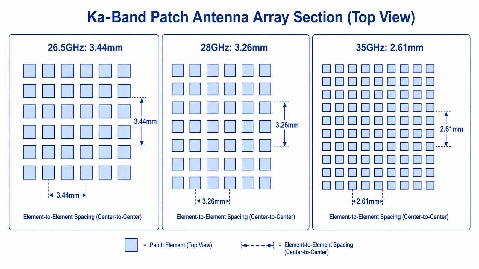
| Frequency | Free-space λ/2 | Effective λ/2 on RO3003 | Design Note |
|---|---|---|---|
| 26.5 GHz | 5.66mm | ~3.44mm | Lower Ka-band edge, more routing room |
| 28 GHz | 5.36mm | ~3.26mm | Common 5G mmWave / satcom Tx frequency |
| 30 GHz | 5.00mm | ~3.04mm | LEO satcom Tx upper range |
| 35 GHz | 4.29mm | ~2.61mm | Ka-band radar, tighter feed routing |
| 40 GHz | 3.75mm | ~2.28mm | Upper Ka-band edge, near RO3003 practical limit |
Element spacing shrinks as frequency increases across the Ka-band range — a phased array designed for 26.5GHz needs roughly 50% more element pitch than one designed for 40GHz. This has direct layout consequences: feed network routing has more available room at the lower end of Ka-band, while designs at the upper edge approach the practical limit of what can be routed on RO3003 at 0.127mm without resorting to multilayer feed distribution. For element spacing and array phase consistency considerations more broadly, see phased array PCB manufacturer.
Loss Budget Across Ka-Band
| Trace Length | RO3003 (Df 0.0010) | RO4003C (Df 0.0027) | RO4350B (Df 0.0037) |
|---|---|---|---|
| 3cm @ 28GHz | ~0.36 dB | ~0.97 dB | ~1.35 dB |
| 5cm @ 28GHz | ~0.60 dB | ~1.61 dB | ~2.25 dB |
| 10cm @ 28GHz | ~1.20 dB | ~3.21 dB | ~4.50 dB |
| 5cm @ 35GHz | ~0.75 dB | ~2.01 dB | ~2.81 dB |
Loss budget calculation at Ka-band should account for the full frequency range your system operates across — a satcom terminal covering both 17.7–20.2GHz (Rx) and 27.5–30GHz (Tx) needs loss verified at the highest frequency in each band, not a single representative point. The difference between RO3003 and RO4003C becomes meaningful at Ka-band: a 5cm trace at 28GHz loses approximately 0.6dB on RO3003 vs 1.6dB on RO4003C — a 1dB difference that matters in a system noise figure budget.
Hybrid Stackup for Satcom Terminal Boards
Satcom terminal designs frequently combine a Ka-band RF front-end (antenna array, LNA/PA interconnect) with lower-frequency control and power layers in a single board. The RF layers use RO3003 for loss and phase performance; control/power layers can use FR4 or RO4350B depending on cost targets and whether any RF content exists on those layers.
- RO3003 RF layers + FR4 control/power layers: bonded with Rogers 2929 bondply at the interface
- Maximum lamination cycles for the full stackup: 2 (set by the PTFE material)
- Layer count for satcom terminal boards commonly ranges 6–16 layers depending on system complexity
TDR impedance verification at multiple Ka-band frequency points — not just one
Via Fence and Ground Isolation at Ka-Band
Via fence spacing for ground isolation follows the same λ/20 guideline used at other mmWave frequencies, but the absolute spacing requirement is somewhat more forgiving than 77GHz due to the lower frequency. At 28GHz, λ/20 spacing works out to approximately 1.34mm — achievable with either laser-drilled microvias or, in some designs, carefully spaced mechanical vias depending on the specific layout constraints. At the upper Ka-band edge (35–40GHz), spacing tightens toward 0.9–1.0mm, where laser drilling becomes the more reliable choice.
Design Checklist for Ka-Band PCB
- Confirm material Dk/Df values used in simulation against actual material certificate at the operating frequency, not nominal datasheet values
- Verify element spacing supports your specific array frequency — recalculate rather than reusing spacing from a different Ka-band design
- Check loss budget at the highest frequency in your operating range, particularly for designs spanning both Rx and Tx Ka sub-bands
- Specify Rogers 2929 bondply explicitly on hybrid stackup drawings — do not leave bonding film unspecified
- Request panel-level Dk uniformity data for large phased array panels where element-to-element phase consistency matters
Ka-Band PCB Design — Q&A
Common questions about material selection, phased array element spacing, loss budget and hybrid stackup design for Ka-band PCB across 26.5–40GHz.
What PCB material is best for Ka-band design?
Rogers RO3003 (Dk 3.0, Df 0.0010) is the standard substrate for most Ka-band applications, offering low loss and tight Dk tolerance needed for both loss budget and phased array phase consistency. For applications without array phase requirements, RO4003C is a cost-effective alternative.
What is the phased array element spacing at 28GHz?
At 28GHz, the effective λ/2 element spacing on RO3003 is approximately 3.26mm. This decreases as frequency increases — at 35GHz it shrinks to ~2.61mm, and at 40GHz to ~2.28mm, requiring progressively tighter feed network routing.
Why does Ka-band loss budget matter more than at lower frequencies?
At 28GHz, a 5cm trace on RO3003 loses ~0.60dB versus 1.61dB on RO4003C — a 1dB difference that directly affects system noise figure. For satcom terminals operating across both Rx and Tx bands, loss budget should be verified at the highest frequency in each band.
What bonding film is used for Ka-band hybrid stackups?
Rogers 2929 bondply is required at the RO3003-to-FR4 interface in hybrid satcom terminal stackups combining Ka-band RF layers with control/power layers. Standard FR4 prepreg should not be used at this interface.
RT5880 In 6 Thicknesses — Lowest Df for Wideband EW
Full thickness range in stock (0.127mm–1.575mm). In-house plasma activation. Single-lot material available for multi-channel array systems. IPC Class 3 on request. 7–10 day prototype, no MOQ.
EW PCB Manufacturer → WhatsAppRequest a PCB Quote
Upload your Gerber ZIP file and project requirements. Our engineering team will review your PCB material, stackup, impedance needs, surface finish, and production quantity before quoting.
Please prepare:
- Gerber files in ZIP format
- PCB material or stackup requirements
- Controlled impedance notes if available
- Prototype or batch production quantity