
PCB-to-Waveguide Transition Design — Microstrip Launch, Loss Budget and Manufacturing Tolerance
As mmWave antenna and interconnect designs push toward W-band and beyond, more systems are combining a standard PCB with a waveguide or 3D-printed metallized waveguide structure rather than relying on a purely planar PCB antenna. The PCB's role in these designs shifts to include a microstrip-to-waveguide transition — a probe structure that couples the RF signal from the PCB trace into the waveguide cavity. This guide covers transition types, the manufacturing tolerances that determine transition loss, and material selection for this application. For general mmWave design background, see our 77GHz radar PCB design guide.
Home » PCB-to-Waveguide Transition Design — Microstrip Launch, Loss Budget and Manufacturing Tolerance
Table of Contents
Why PCB + Waveguide Hybrid Structures Are Growing
A pure planar PCB antenna becomes increasingly lossy and difficult to fabricate reliably as frequency climbs into W-band and beyond — trace dimensions shrink to fractions of a millimeter, and fabrication tolerance becomes a larger fraction of the electrical wavelength. Waveguide structures, particularly metallized molded plastic waveguides, offer lower loss and easier scaling to very high frequencies for the antenna and feed structure itself. This does not eliminate the PCB — the MMIC, power supply, control circuitry and the transition structure that couples the two domains together still require a PCB, but the PCB’s role becomes more specialized around that transition.
Transition Types and Loss
| Transition Type | Frequency Range | Typical Insertion Loss | Manufacturing Complexity |
|---|---|---|---|
| Microstrip probe (E-plane probe) | 24–110GHz | 0.3–0.8dB per transition | Moderate — standard PCB fabrication |
| Microstrip-to-ridge waveguide | 40–110GHz | 0.2–0.6dB per transition | Moderate to high — tight probe geometry |
| SIW to standard waveguide | 30–100GHz | 0.3–0.7dB per transition | High — requires via wall fence around SIW section |
| Direct microstrip-to-horn (radiating) | 60–100GHz | Application-dependent | Moderate — geometry tied to antenna pattern |
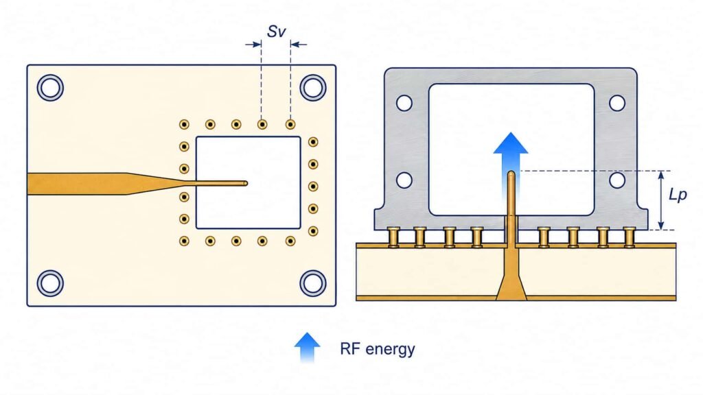
The probe-based transition (E-plane probe) is the most common approach for coupling a microstrip trace into a rectangular waveguide — a small probe structure extends into the waveguide opening, launching the RF energy from the guided microstrip mode into the waveguide’s propagating mode. SIW (Substrate Integrated Waveguide) transitions use a via-fenced region on the PCB itself to approximate waveguide behavior before transitioning to a true metal waveguide, which can simplify the mechanical interface at the cost of additional PCB-side design complexity.
Manufacturing Tolerance at the Transition
| Parameter | Standard Tolerance | Impact if Out of Spec |
|---|---|---|
| Probe length and position | ±0.05mm typical | Direct source of return loss degradation |
| Waveguide alignment to PCB probe | ±0.05–0.1mm mechanical | Misalignment couples energy poorly |
| Via fence around SIW section | ≤λ/10, laser-drilled at mmWave | Wider spacing leaks energy through walls |
| Substrate thickness at transition | Tight, material-dependent | Thickness variation shifts probe behavior |
| Copper thickness/roughness at probe | Confirm against EM simulation | Roughness affects loss more at mmWave |
The transition is typically the single most tolerance-sensitive feature on a PCB-to-waveguide design. Probe position error of even 0.05mm can measurably shift the transition’s return loss at W-band frequencies, where the electrical wavelength is only a few millimeters. Confirm your fabricator’s actual achievable tolerance for probe geometry and position — not just their standard trace/space tolerance — before finalizing a transition design based on simulation alone.
Material Selection for Transition Designs
| Application | Frequency | Recommended Substrate | Reason |
|---|---|---|---|
| 77/79GHz automotive radar w/ waveguide antenna | 76–81GHz | Rogers RO3003 0.127mm | Standard automotive substrate, thin geometry for probe |
| E-band backhaul (71–86GHz) | 71–86GHz | Rogers RT5880 0.127mm | Lowest Df, wider trace for lower conductor loss |
| W-band sensing/imaging | 75–110GHz | Rogers RT5880 0.127mm | Only standard material with acceptable loss |
| SIW-based transitions (lower mmWave) | 24–40GHz | Rogers RO3003 0.254mm | Thicker substrate feasible, easier via fence spacing |
Substrate thickness at the transition point directly affects the probe’s electrical behavior, since the probe geometry is typically optimized in simulation against a specific substrate thickness and Dk. See our Rogers RO3003 PCB guide and Rogers RT5880 PCB guide for available thickness options — confirm your target thickness is available as standard stock before finalizing a transition design around it, since custom thicknesses can add material lead time.
Mechanical Alignment Between PCB and Waveguide
Beyond the PCB’s own fabrication tolerance, the mechanical alignment between the PCB probe and the mating waveguide flange is a system-level tolerance stack that the PCB fabricator alone cannot fully control. Confirm mounting hole position tolerance and board outline tolerance at the transition area specifically — these mechanical tolerances, not just the electrical trace geometry, determine whether the probe actually lands in the correct position relative to the waveguide opening once assembled.
DFM Checklist for PCB-to-Waveguide Transitions
- Confirm probe geometry tolerance achievable by your fabricator — request this explicitly, not as an assumed extension of standard trace tolerance
- Specify via fence spacing for any SIW section — see via design for RF PCBfor the λ/10 spacing rule and how it scales at mmWave frequencies
- Confirm substrate thickness at the transition matches your simulation model exactly — request material lot certificate with actual thickness data
- Specify mounting hole and board outline tolerance at the transition area explicitly on the mechanical drawing
- Request a test coupon with the transition structure for pre-production verification if system-level phase or loss performance is critical
PCB-to-Waveguide Transition Design — Q&A
Common questions about waveguide transition types, manufacturing tolerance, and material selection for mmWave applications.
What is a PCB-to-waveguide transition?
A probe structure on a PCB that couples RF energy from a microstrip trace into a waveguide cavity. The most common type is an E-plane probe, used from ~24GHz to 110GHz where a system combines PCB circuitry with a waveguide antenna or feed.
Why are PCB-to-waveguide transitions becoming more common in radar design?
As mmWave designs push toward W-band, purely planar PCB antennas become lossy and difficult to fabricate reliably at very small dimensions. Waveguide structures offer lower loss at high frequencies, while the PCB retains MMIC, power, and control circuitry connected via a transition.
What manufacturing tolerance is required for a waveguide probe transition?
Probe position and length tolerance around ±0.05mm typically, since small errors can measurably shift return loss at W-band where the electrical wavelength is only a few millimeters. Substrate thickness accuracy is equally important.
PCB-to-Waveguide Transitions — Test Coupon Verification Available
Rogers RO3003 and RT5880 in 0.127mm for W-band probe geometry. Laser microvia to 0.10mm for SIW via fence. Material lot thickness certificates. Test coupon fabrication for pre-production verification.
77GHz Radar PCB Manufacturer → WhatsAppRequest a PCB Quote
Upload your Gerber ZIP file and project requirements. Our engineering team will review your PCB material, stackup, impedance needs, surface finish, and production quantity before quoting.
Please prepare:
- Gerber files in ZIP format
- PCB material or stackup requirements
- Controlled impedance notes if available
- Prototype or batch production quantity