Rogers RO4350B is the most widely used high frequency PCB material in the world. More RF and microwave circuit boards are built on RO4350B than on any other Rogers laminate — and for good reason. It delivers RF performance significantly better than FR4 while processing on standard FR4-compatible manufacturing equipment. This combination of electrical performance and manufacturing compatibility is what made RO4350B the default material for a generation of RF PCB design.
As a direct Rogers PCB factory with RO4350B in production inventory across the full standard thickness range, we build RO4350B PCB every week — from simple 2-layer RF test boards to complex 16-layer hybrid stackups for aerospace applications. This guide covers everything engineers and buyers need to know about specifying, designing, and manufacturing Rogers RO4350B PCB.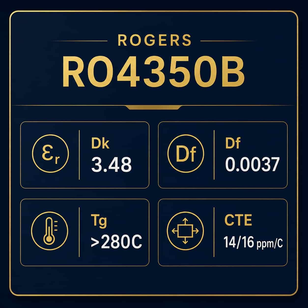
Quick Summary: Rogers RO4350B at a Glance
Key point: Rogers RO4350B (Dk 3.48 ±0.05, Df 0.0037 at 10 GHz, Tg >280°C) is the standard RF PCB material for applications from L-band through X-band. It processes on FR4-compatible equipment — no plasma activation, no special bonding film chemistry beyond Rogers RO4450F, no PTFE-specific drill parameters. This makes it available from more factories at lower cost than Rogers PTFE materials while delivering RF performance 5× better than FR4. The main limitation is Df: at Ka-band and above, or in wide-band EW systems, Rogers RO3003 or RT5880 provide meaningfully lower loss.
Rogers RO4350B Material Properties
Understanding the key material properties of RO4350B is the foundation for correct application of this material in RF PCB design. The following properties are the ones that matter most for design and manufacturing decisions.
Dielectric Constant (Dk)
- Nominal Dk: 3.48 at 10 GHz — the value used for impedance calculations
- Dk tolerance: ±0.05 — production Dk may be 3.43 to 3.53
- Dk frequency dependence: Dk decreases slightly with frequency — 3.66 at 1 GHz, 3.48 at 10 GHz, approximately 3.4 at 20 GHz
- Dk temperature coefficient: +50 ppm/°C — Dk increases slightly with temperature
- Production Dk vs nominal: our factory uses the confirmed lot Dk from the Rogers material certificate for impedance calculation — not the nominal 3.48
Why production Dk matters: A Rogers material certificate may show a confirmed production Dk of 3.51 for a specific lot. Using 3.48 for impedance calculation on that lot produces a trace width that is slightly too narrow, shifting the impedance by approximately 0.5%. For most designs this is within tolerance. For tight-budget designs, using the confirmed lot Dk provides the most accurate impedance.
Dissipation Factor (Df)
- Df at 10 GHz: 0.0037 — approximately 5× lower than standard FR4 (0.020)
- Df at 2.4 GHz: approximately 0.0037 — relatively stable at lower frequencies
- Df at 24 GHz: approximately 0.0040 — slight increase at higher frequencies
- Insertion loss at 10 GHz: approximately 0.35 dB/inch on 0.508mm substrate with 1 oz copper microstrip
- Comparison: Rogers RO4003C Df 0.0027 — 27% lower than RO4350B
- Comparison: Rogers RO3003 Df 0.0010 — 73% lower than RO4350B
Thermal Properties
- Glass transition temperature (Tg): >280°C — far above any PCB operating temperature
- Decomposition temperature (Td): >280°C — material does not degrade at solder reflow temperatures
- Coefficient of thermal expansion (CTE) x-axis: 14 ppm/°C
- CTE y-axis: 16 ppm/°C — close to copper (17 ppm/°C), good dimensional stability
- CTE z-axis: 32–46 ppm/°C — acceptable for most PCB layer counts
- Thermal conductivity: 0.69 W/m·K — higher than standard FR4 (0.25 W/m·K)
Mechanical Properties
- Flexural strength: 276 MPa — rigid material, not suitable for flex applications
- Young’s modulus: 19.0 GPa — stiffer than FR4
- Moisture absorption: 0.06% — very low, good stability in humid environments
- Density: 1.86 g/cm³ — similar to FR4
Why Rogers RO4350B Became the Standard RF PCB Material
The dominance of Rogers RO4350B in the RF PCB market is not accidental. It is the result of a specific engineering trade-off that RO4350B solved better than any alternative available when it was introduced: delivering PTFE-class RF performance using FR4-class manufacturing processes.
- Before RO4350B: engineers choosing a high frequency laminate had to choose between FR4 (cheap, easy to process, poor RF performance) and PTFE materials (excellent RF performance, expensive, difficult to process — requiring plasma activation and specialized drill parameters)
- RO4350B’s solution: a hydrocarbon ceramic composite that achieves Df of 0.0037 — far better than FR4’s 0.020 — while processing on standard FR4 equipment without plasma activation or special drill parameters
- The result: factories that were already building FR4 PCB could start building Rogers RO4350B with modest process adjustments — primarily adding Rogers RO4450F bondply to inventory and adjusting lamination temperature profiles
- Network effect: as more factories adopted RO4350B, availability increased and price decreased — further cementing its position as the default RF material
- Today: RO4350B is specified in more RF PCB programs globally than any other Rogers material — from 5G base station antennas to aerospace radar to automotive ADAS sensors
Impedance Calculation for Rogers RO4350B PCB
Controlled impedance is a fundamental requirement for most RO4350B PCB designs. The 50Ω microstrip is the most common transmission line structure. The trace width for 50Ω depends on the substrate thickness, copper weight, and confirmed production Dk.
50Ω Microstrip Trace Width on RO4350B
The following trace widths achieve 50Ω characteristic impedance on Rogers RO4350B with 1 oz (35 µm) finished copper on the outer layer. These are calculated using Dk 3.48 (nominal) — actual production may vary slightly based on lot Dk from material certificate.
- RO4350B 0.127 mm substrate: 50Ω trace width ≈ 0.25 mm (10 mil)
- RO4350B 0.254 mm substrate: 50Ω trace width ≈ 0.51 mm (20 mil)
- RO4350B 0.338 mm substrate: 50Ω trace width ≈ 0.69 mm (27 mil)
- RO4350B 0.508 mm substrate: 50Ω trace width ≈ 1.08 mm (43 mil)
- RO4350B 0.762 mm substrate: 50Ω trace width ≈ 1.65 mm (65 mil)
- RO4350B 1.524 mm substrate: 50Ω trace width ≈ 3.35 mm (132 mil)
Important: These are calculated values using nominal Dk 3.48. Our factory recalculates impedance for every order using the confirmed production Dk from the Rogers material certificate for that specific lot. If the lot Dk is 3.51 instead of 3.48, the required trace width for 50Ω shifts by approximately 0.4%. For most designs this is within the ±10% impedance tolerance, but we report it in DFM feedback so the designer can decide whether to adjust.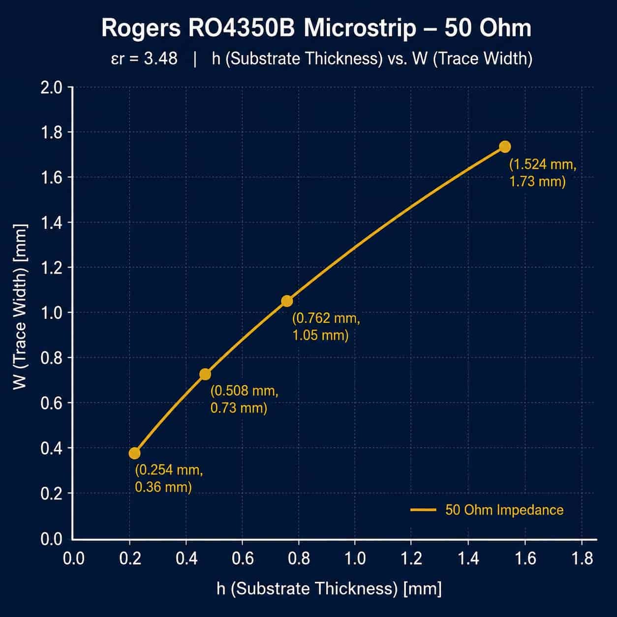
100Ω Differential Pair on RO4350B
- RO4350B 0.254 mm substrate: 100Ω differential pair trace width ≈ 0.28 mm (11 mil), gap ≈ 0.15 mm (6 mil)
- RO4350B 0.508 mm substrate: 100Ω differential pair trace width ≈ 0.65 mm (26 mil), gap ≈ 0.20 mm (8 mil)
- These are approximate — actual values depend on trace geometry and coupling
Impedance Tolerance
- Standard impedance tolerance: ±10% — confirmed by TDR measurement on every production lot
- Advanced impedance tolerance: ±8% — available on request, same TDR verification
- Coupon: impedance test coupon placed on panel edge — TDR measurement records available on request
Stackup Design for Rogers RO4350B PCB
The stackup design determines the achievable impedance, board thickness, layer count, and cost. The following are the most common RO4350B stackup configurations used in production.
2-Layer RO4350B Stackup
The simplest RO4350B stackup — RF signal on top layer, continuous ground plane on bottom. Used for simple RF test boards, filter PCB, and modules where routing complexity is low.
- Layer 1: RO4350B, 0.508 mm, 1 oz copper — RF signal layer
- Layer 2: 1 oz copper — continuous ground plane
- Total thickness: approximately 0.58 mm
- Applications: RF test circuits, filters, simple antenna feed networks
- Limitation: no power plane, no signal isolation between layers
4-Layer RO4350B Stackup (Full Rogers)
The standard 4-layer RO4350B stackup for RF PCB with power distribution and signal isolation requirements.
- Layer 1: RO4350B 0.508 mm, 1 oz — RF signal, antenna feed
- Bondply: Rogers RO4450F 0.101 mm
- Layer 2: 1 oz copper — continuous ground plane
- Core: RO4350B 0.508 mm
- Layer 3: 1 oz copper — power plane
- Bondply: Rogers RO4450F 0.101 mm
- Layer 4: RO4350B 0.508 mm, 1 oz — bottom signal layer
- Total thickness: approximately 1.57 mm
4-Layer Hybrid RO4350B + FR4 Stackup
The most cost-effective approach for RF PCB with digital sections — Rogers on the RF signal layer, FR4 on the other layers.
- Layer 1: RO4350B 0.254 mm, 1 oz — RF signal layer (Rogers required here only)
- Bondply: Rogers RO4450F 0.101 mm
- Layer 2: 1 oz copper — ground plane
- Core: FR4 0.762 mm (high-Tg FR4 recommended)
- Layer 3: 1 oz copper — power / digital signal
- Prepreg: FR4 standard prepreg 0.101 mm
- Layer 4: 1 oz copper — bottom digital routing
- Total thickness: approximately 1.6 mm
- Cost saving: approximately 30–40% vs full Rogers construction
- Key requirement: Rogers RO4450F bondply at the Rogers-FR4 interface — not standard FR4 prepreg
For hybrid stackup design details, see Mixed Laminate High Frequency PCB: How FR4 and Rogers Are Combined in Production.
Multilayer RO4350B Stackup
For complex RF PCB with multiple signal layers, power distribution, and digital sections — 8, 12, or 16 layers.
- RF signal layers: RO4350B — only on layers requiring RF performance
- Ground and power planes: can use FR4 core or RO4350B depending on cost and performance requirements
- Bonding film: Rogers RO4450F at all Rogers-to-Rogers and Rogers-to-FR4 interfaces
- Maximum lamination cycles: 3 for RO4350B — allows complex multilayer structures
- Layer count: 2–32 standard, up to 50 advanced
For multilayer stackup guidance, see Multilayer High Frequency PCB: Layer Count, Stackup and Manufacturing Limits.
Rogers RO4350B Manufacturing Process
The FR4-compatible processing of Rogers RO4350B is its defining manufacturing advantage. Understanding what this means in practice helps verify that a factory can reliably produce RO4350B PCB.
What FR4-Compatible Means
- No plasma activation required: RO4350B hole walls bond to electroless copper without special surface treatment — unlike Rogers RO3003 and RT5880 which require plasma or sodium activation
- Standard drill parameters: RO4350B can be drilled with the same spindle speed and feed rate as FR4 — no PTFE-specific parameters needed
- Standard desmear: permanganate desmear process works for RO4350B — no special chemistry
- Standard lamination equipment: same press as FR4 — different temperature profile, same equipment
- Maximum 3 lamination cycles: same as high-performance FR4
What RO4350B Requires That FR4 Does Not
- Rogers RO4450F bondply: the bonding film for RO4350B hybrid stackups must be Rogers RO4450F or RO4450T — not standard FR4 prepreg. Using FR4 prepreg at the Rogers-FR4 interface creates an impedance discontinuity. Ask the factory to confirm RO4450F is in inventory before ordering.
- Adjusted lamination temperature profile: RO4350B requires a different press temperature cycle than FR4 — a factory that has never built RO4350B may need process development before first production
- Impedance calculation with Rogers Dk: the factory must calculate impedance using the confirmed RO4350B production Dk — not generic FR4 Dk values
Drilling Capability for RO4350B
- Minimum mechanical drill diameter: 0.2 mm standard, 0.1 mm advanced
- Aspect ratio: 10:1 standard, 14:1 advanced
- Hole position tolerance: ±0.075 mm standard, ±0.05 mm advanced
- No PTFE-specific requirements — standard FR4 drill parameters work
For drilling capability details, see Drilling Capabilities for High Frequency PCB.
Rogers RO4350B PCB Applications by Frequency Band
L-Band and S-Band (1–4 GHz): Surveillance Radar, 5G Sub-6, IFF
At L-band and S-band, RO4350B’s Df of 0.0037 provides ample performance advantage over FR4. Insertion loss at these frequencies is low enough that even long feed networks — 300–500 mm on large phased array panels — remain within link budgets.
- 5G massive MIMO base station antenna (3.5 GHz): RO4350B on large panels up to 480×800 mm
- S-band naval surveillance radar: RO4350B — standard choice for production naval arrays
- L-band IFF interrogator: RO4350B — adequate Df at 1–1.2 GHz
- Air traffic control radar (S-band): RO4350B
- WiFi 2.4 GHz and 5 GHz modules: RO4350B or F4B for cost-sensitive designs
C-Band and X-Band (4–12 GHz): Weather Radar, Fire Control, Satellite
At C-band and X-band, RO4350B remains the standard choice for most applications. The exception is X-band fire control radar with very long feed networks, where RO4003C’s lower Df provides a meaningful link margin advantage.
- Weather radar (C-band, 5.6 GHz): RO4350B — standard material for meteorological radar
- Maritime navigation radar (X-band, 9.4 GHz): RO4350B — widely used in commercial marine radar
- X-band fire control radar (short feed network): RO4350B — adequate for compact arrays
- Ku-band VSAT terminal (10.7–12.75 GHz): RO4350B for most commercial terminal designs
- Point-to-point microwave link (6–11 GHz): RO4350B
When to Upgrade from RO4350B
RO4350B is not the correct choice for every application. Two scenarios consistently justify upgrading to RO4003C or RO3003:
- Long feed networks at X-band: if the RF path from the transmitter to the antenna element exceeds 150–200 mm at 10 GHz, calculate the insertion loss for both RO4350B (Df 0.0037) and RO4003C (Df 0.0027). If RO4350B exceeds the system loss budget, upgrade to RO4003C.
- Ka-band designs (26.5 GHz+): at Ka-band, RO4350B Df produces significantly more insertion loss than RO3003. For antenna element dimensions at 35 GHz on RO4350B, the trace widths and element sizes are also larger than on RO3003 due to higher Dk. Upgrade to Rogers RO3003.
- Wideband EW (2–18 GHz): RO4350B Dk stability over the full EW band is insufficient for sensitive receivers — use Rogers RT5880.
- W-band (75–110 GHz): RO4350B is not suitable — Rogers RT5880 only.
For the full Rogers material selection guide, see Rogers PCB Material Selection Guide. For RO4350B vs RO4003C vs RO3003 comparison, see Rogers PCB vs PTFE PCB: Which High Frequency Material Is Right?.
Rogers RO4350B vs Alternatives
RO4350B vs RO4003C
- Dk: RO4350B 3.48, RO4003C 3.38 — slightly different, trace widths will differ
- Df: RO4350B 0.0037, RO4003C 0.0027 — RO4003C has 27% lower insertion loss
- Processing: identical — same FR4-compatible equipment, same RO4450F bondply
- Cost: RO4003C approximately 20–35% more expensive than RO4350B
- When to choose RO4003C: X-band designs with long feed networks, Ku-band, or when insertion loss budget is tight
RO4350B vs Taconic RF-35
- Dk: RO4350B 3.48, Taconic RF-35 3.50 — essentially identical
- Df: RO4350B 0.0037, Taconic RF-35 0.0018 — RF-35 has 51% lower Df
- Processing: RO4350B is FR4-compatible; RF-35 is PTFE and requires plasma activation
- When to choose RF-35: commercial RF designs below 20 GHz where Rogers documentation is not required and a factory with PTFE capability is available
RO4350B vs Isola Astra MT77
- Dk: RO4350B 3.48, Astra MT77 3.04 — different Dk means different trace widths
- Df at 10 GHz: RO4350B 0.0037, Astra MT77 0.0017 — Astra MT77 has lower Df at 10 GHz
- Tg: RO4350B >280°C, Astra MT77 190°C — RO4350B has much higher Tg
- Dk temperature stability: RO4350B +50 ppm/°C, Astra MT77 ~+100 ppm/°C — RO4350B more stable
- When to choose Astra MT77: commercial RF below 15 GHz where Rogers certification is not required and cost saving is a priority
For Isola vs Rogers comparison, see Isola vs Rogers: Which High Frequency PCB Material Is Right for Your Application?.
Surface Finish for Rogers RO4350B PCB
- ENIG (Electroless Nickel Immersion Gold): standard for most RO4350B designs — flat surface, good solderability, suitable to X-band. Nickel layer adds slight resistance at frequencies above 10 GHz but acceptable for most RO4350B applications.
- ENEPIG: preferred for aerospace and defense IPC Class 3 programs — eliminates black pad risk. Recommended when RO4350B is used in applications with high reliability requirements.
- Immersion Silver: preferred above 10 GHz where pad resistance matters — silver deposits directly on copper with no nickel layer. Good choice for Ku-band VSAT and X-band designs with tight RF budget.
- OSP: not recommended for RF PCB — uneven surface and limited shelf life affect impedance control.
For surface finish selection details, see ENIG vs ENEPIG vs Immersion Silver for High Frequency PCB.
Rogers RO4350B Production at Riching PCB
As a direct Rogers PCB factory, we hold Rogers RO4350B in production inventory across the full standard thickness range. RO4350B is our highest-volume Rogers material — we build it in regular production every week.
RO4350B Inventory
- Standard thicknesses in inventory: 0.101 mm / 0.168 mm / 0.254 mm / 0.338 mm / 0.422 mm / 0.508 mm / 0.762 mm / 1.524 mm
- Non-standard thicknesses: available by special order — confirm availability and lead time before design finalization
- Copper foil: standard electrolytic copper (ED) — rolled annealed (RA) available on request
- Rogers RO4450F bondply: in stock for hybrid stackup production
Manufacturing Specifications for RO4350B
- Controlled impedance: ±10% standard, ±8% advanced — TDR verified on every production lot
- Impedance calculation: using confirmed production Dk from Rogers material certificate lot
- Minimum outer layer line width: 2.5 mil advanced, 3 mil standard
- Minimum drill diameter: 0.1 mm advanced, 0.2 mm standard
- Maximum aspect ratio: 14:1 advanced, 10:1 standard
- Layer count: 2–32 standard, up to 50 advanced
- Maximum lamination cycles: 3
- IPC Class: Class 2 standard, Class 3 available for aerospace and defense
- Material certificates: Rogers-certified with lot numbers — available for all RO4350B production
- Lead time: standard 5–7 working days for 2–4 layer prototype; 10–15 days for complex multilayer
What to Prepare for Rogers RO4350B PCB Quotation
- Gerber files — all copper layers, solder mask, board outline
- NC drill file — all hole sizes, PTH and NPTH separated
- Stackup drawing — RO4350B grade confirmed, dielectric thickness and copper weight per layer
- RO4350B substrate thickness — specify from standard range or confirm special order availability
- Controlled impedance — target value, tolerance, layer, trace structure
- Board dimensions and quantity
- Surface finish — ENIG, ENEPIG, or immersion silver
- IPC Class — Class 2 or Class 3
- Application type — commercial, aerospace, defense, automotive
- Rogers-certified material certificate requirement — specify if needed for program
- Delivery requirement
For the complete quotation file checklist, see What Files Are Needed for a High Frequency PCB Quotation?.
Conclusion
Rogers RO4350B is the dominant RF PCB material because it solves the core problem of high frequency PCB: delivering RF performance far better than FR4 while processing on equipment that FR4 factories already have. Dk 3.48 ±0.05, Df 0.0037, Tg >280°C, and FR4-compatible manufacturing make it the correct first choice for RF and microwave PCB from L-band through X-band across commercial, aerospace, and defense applications.
The only situations where RO4350B is not the correct choice are: Ka-band and above (upgrade to Rogers RO3003), wide-band EW covering 2–18 GHz (upgrade to RT5880), and X-band designs where long feed networks push the insertion loss beyond budget (upgrade to RO4003C). For everything else, RO4350B is the place to start. As a direct Rogers PCB factory with RO4350B in regular production inventory, we review every RO4350B order with our engineering team before production — confirming impedance using lot Dk, stackup feasibility, and bonding film availability before your design is committed to production.