Rogers RT5880 PCB: Lowest Loss PTFE Glass for EW, mmWave and Wideband RF
Complete guide to Rogers RT5880 — Dk 2.20, Df 0.0009. Standard substrate for wideband EW 2–18 GHz, Ka-band, and W-band applications. Available thicknesses 0.127–3.175 mm, 50Ω trace widths, in-stock availability and manufacturing requirements.
Home » EW PCB material » Rogers RT5880 PCB: Lowest Loss PTFE Glass for EW, mmWave and Wideband RF
Table of Contents
Key point: Most factories quote 3–4 weeks waiting for RO3003 / RT5880 material procurement. Riching PCB maintains these materials in stock — no material wait.Rogers RT5880 is the lowest-loss standard Rogers material — Dk 2.20, Df 0.0009. Standard for wideband EW 2–18 GHz, W-band (75–110 GHz), and Ka-band applications requiring minimum insertion loss. 50Ω microstrip on 0.508 mm RT5880 with 1 oz copper: ~1.51 mm trace width. Available thicknesses: 0.127 / 0.254 / 0.381 / 0.508 / 0.787 / 1.575 / 3.175 mm. RT5880 costs USD 800–1,500/m² — most factories do not stock it, quoting 3–4 weeks for material procurement. Riching PCB maintains RT5880 in stock across 6 standard thicknesses with in-house plasma activation — 7–10 working day prototype, no MOQ, no material wait.
Rogers RT5880 is the lowest-loss standard Rogers material — Df 0.0009 at 10 GHz, lower than any other Rogers substrate including RO3003. It is a PTFE glass laminate, one of the oldest and most reliable microwave PCB substrates, and remains the standard choice for wideband electronic warfare systems covering 2–18 GHz and beyond. RT5880 is also widely used for W-band (75–110 GHz) applications where its Dk stability across a wide frequency and temperature range is critical.
This guide covers RT5880 material properties, available thicknesses, 50Ω microstrip trace widths, comparison with RO3003, manufacturing requirements, and applications.
RT5880 Material Properties
| Property | Value | Test Condition |
|---|---|---|
| Dielectric Constant (Dk) | 2.20 ± 0.02 | 10 GHz, IPC-TM-650 2.5.5.5 |
| Dissipation Factor (Df) | 0.0009 — lowest of any standard Rogers material | 10 GHz, IPC-TM-650 2.5.5.5 |
| TCDk | –125 ppm/°C | –50 to +150°C |
| Thermal Conductivity | 0.20 W/m/K | ASTM C518 |
| CTE (x, y axis) | 31 ppm/°C | IPC-TM-650 2.4.41 |
| CTE (z axis) | 237 ppm/°C | IPC-TM-650 2.4.41 |
| Tg | >500°C (PTFE) | — |
| Flame Retardant | UL 94 V-0 | — |
| Process Type | PTFE glass — plasma activation required | — |
The TCDk of –125 ppm/°C is notably larger in magnitude than RO3003 (+13 ppm/°C). This means RT5880 Dk changes more with temperature — a relevant consideration for designs requiring tight resonance stability over wide temperature ranges. For most commercial EW and mmWave applications operating from –40°C to +85°C, the total Dk shift is approximately 0.014 — acceptable for ±10% impedance tolerance designs.
RT5880 vs RO3003: When to Choose Each
| Material | Dk | Df | Type | Best Use Case |
|---|---|---|---|---|
| RT5880 | 2.20 | 0.0009 | PTFE glass | Wideband EW 2–18 GHz, lowest loss, W-band |
| RT5870 | 2.33 | 0.0012 | PTFE glass | Slightly higher Dk, same process as RT5880 |
| RO3003 | 3.0 | 0.0010 | PTFE ceramic | Ka-band, 77 GHz — better thermal, smaller elements |
| RO4350B | 3.48 | 0.0037 | Hydrocarbon | RF below 12 GHz, FR4-compatible process |
| Taconic TLY-5 | 2.17 | 0.0009 | PTFE glass | RT5880 equivalent, cost alternative |
The choice between RT5880 and RO3003 comes down to three factors:
1. Insertion Loss Priority → RT5880
RT5880 Df 0.0009 is 10% lower than RO3003 Df 0.0010. At 18 GHz over a 10 cm trace, this represents approximately 0.2 dB less insertion loss — meaningful for wideband EW systems where every dB in the RF chain matters. For wideband ESM receivers covering 2–18 GHz, RT5880 is the standard choice.
2. Wideband Coverage → RT5880
RT5880’s Dk remains stable from 1 GHz to 40 GHz and beyond — its low Dk (2.20) and woven glass construction produce minimal frequency-dependent variation. For designs requiring consistent performance across an octave or more of bandwidth, RT5880 outperforms RO3003.
3. Thermal Management → RO3003
RO3003 thermal conductivity 0.50 W/m/K vs RT5880 0.20 W/m/K — RO3003 dissipates heat 2.5× more effectively. For high-power phased arrays with integrated beamforming ICs generating significant heat, RO3003 is the better choice. For passive RF circuits and EW receivers where thermal management is less critical, RT5880 is preferred.
Available Thicknesses and 50Ω Microstrip Trace Widths
RT5880 standard dielectric thicknesses: 0.127 mm / 0.254 mm / 0.381 mm / 0.508 mm / 0.787 mm / 1.575 mm / 3.175 mm
RT5880 has the widest thickness range of any Rogers PTFE material — 7 standard options from 0.127 mm to 3.175 mm. The 3.175 mm option is unique to RT5880 and RT5870 within the Rogers PTFE range, useful for lower-frequency applications requiring thick substrate.
| Core Thickness | Copper Weight | 50Ω Microstrip Width (approx.) | Typical Application |
|---|---|---|---|
| 0.127 mm | 0.5 oz | ~0.35 mm | Ka-band 28 GHz, 77 GHz |
| 0.254 mm | 1 oz | ~0.74 mm | Ka-band feed network, EW |
| 0.381 mm | 1 oz | ~1.12 mm | Ku-band, wideband EW |
| 0.508 mm | 1 oz | ~1.51 mm | EW 2–18 GHz standard thickness |
| 0.787 mm | 1 oz | ~2.35 mm | Lower frequency wideband |
| 1.575 mm | 1 oz | ~4.73 mm | Lower frequency RF |
| 3.175 mm | 1 oz | ~9.52 mm | Thick substrate applications |
Approximate values. Confirm with fabricator using production Dk from material certificate.
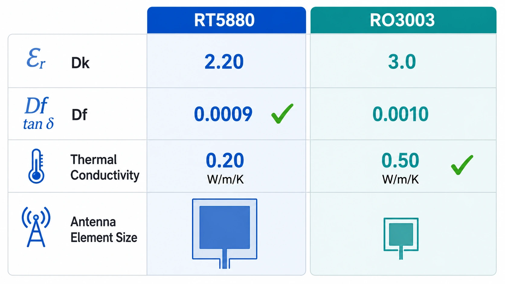
Note: RT5880 lower Dk (2.20) produces wider traces than RO3003 (3.0) for the same impedance and thickness. On 0.508 mm with 1 oz copper: RT5880 ~1.51 mm vs RO3003 ~1.25 mm. This wider trace is easier to manufacture at minimum line width — a practical advantage for wideband designs.
Why Most Factories Don’t Stock RT5880
RT5880 costs approximately USD 800–1,500 per square meter of raw laminate — 5–10× more than RO4350B and significantly more than RO3003. Combined with PTFE-specific process requirements (plasma activation, special drill parameters, 2-cycle lamination limit), most PCB factories treat RT5880 as a special-order material requiring 3–4 weeks for material procurement plus manufacturing.
Riching PCB maintains RT5880 in stock across multiple standard thicknesses — 0.127 mm, 0.254 mm, 0.381 mm, 0.508 mm, 0.787 mm, 1.575 mm — as a standard inventory item. This eliminates the material procurement delay and enables 7–10 working day prototype lead time from design submission to shipping, compared to 4–6 weeks at most Chinese factories and Western fabricators.
Manufacturing Requirements
Plasma Activation — Same as All PTFE
RT5880 is PTFE glass and requires in-house plasma or sodium naphthalene hole wall activation before copper plating — identical requirement to RO3003. See PTFE PCB manufacturing challenges for full process detail.
Maximum 2 Lamination Press Cycles
RT5880 is limited to 2 lamination press cycles — same as all Rogers PTFE materials. Multi-layer RT5880 hybrid stackups with FR4 inner layers use Rogers 4450F or equivalent bondply at the RT5880/FR4 interface.
CTE Mismatch in Hybrid Stackups
RT5880 z-axis CTE (237 ppm/°C) is significantly higher than FR4 (50–70 ppm/°C). In hybrid stackups, this CTE mismatch can cause via barrel fatigue under thermal cycling for through-hole vias spanning the RT5880 layer. For high-reliability applications, use blind vias in the RT5880 layer rather than through-hole vias spanning the full stackup.
Copper Foil
For EW and mmWave applications, low-profile (LP) copper foil reduces surface roughness contribution to insertion loss. RT5880 benefits more from LP copper than most materials because its intrinsic Df is already at 0.0009 — at this loss level, copper surface roughness becomes a significant fraction of total insertion loss.
Applications
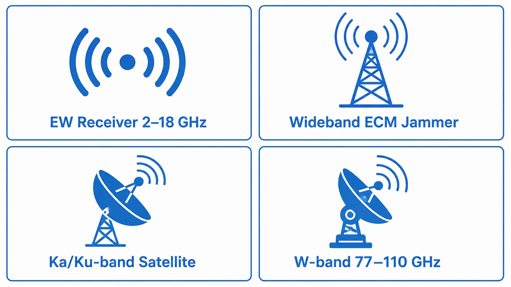
- Wideband EW PCB— ESM receiver and ECM jammer 2–18 GHz (primary application)
- W-band PCB (75–110 GHz) — automotive radar, imaging radar, point-to-point backhaul
- Ka-band satellite terminal PCB— where maximum insertion loss reduction is required
- 5G mmWave PCB— n260 band (37–40 GHz) where RT5880 outperforms RO3003
- DRFM (Digital Radio Frequency Memory) — wideband signal capture and replay
- Wideband power amplifier and LNA PCB — 2–40 GHz
- Satellite payload RF PCB — where weight and insertion loss are primary constraints
Conclusion
Rogers RT5880 (Dk 2.20, Df 0.0009) is the lowest-loss standard Rogers material and the first choice for wideband EW systems (2–18 GHz), W-band applications, and any design where minimum insertion loss is the priority. It requires in-house plasma activation, max 2 lamination cycles, and is significantly more expensive than RO4350B or RO3003 — most factories do not stock it. Riching PCB maintains RT5880 in stock across 6 standard thicknesses with in-house plasma activation, enabling 7–10 working day prototype vs 4–6 weeks at most suppliers. No MOQ. See Rogers materials overview for full thickness availability.
Order Rogers RT5880 PCB — In Stock, No Wait
RT5880 in stock: 0.127 / 0.254 / 0.381 / 0.508 / 0.787 / 1.575 mm. In-house plasma activation. 7–10 day prototype. Send the following:
- Gerber files + NC drill file
- RT5880 dielectric thickness
- Copper weight per layer
- Controlled impedance target and tolerance
- Operating frequency and application type
- IPC Class and quantity
WhatsApp +86 13760473650 — DFM review within 24 hours
Rogers RT5880 PCB Q&A
Common questions about Rogers RT5880 applications, differences from RO3003, available thicknesses, sourcing and plasma activation requirements.
What is Rogers RT5880 used for?
Standard for wideband EW 2–18 GHz (primary application), W-band 75–110 GHz, Ka-band minimum-loss designs, and 5G n260 band 37–40 GHz. Lowest-loss standard Rogers material — the first choice when wideband frequency coverage and minimum insertion loss are both required.
What is the difference between RT5880 and RO3003?
RT5880 Dk 2.20, Df 0.0009 — lower Df, lower Dk, lower thermal conductivity (0.20 vs 0.50 W/m/K). Lower Dk means ~17% larger antenna elements. RO3003 preferred for high-power phased arrays (better heat spreading). RT5880 preferred for EW, wideband, minimum-loss applications.
What thicknesses are available for Rogers RT5880?
7 options: 0.127 / 0.254 / 0.381 / 0.508 / 0.787 / 1.575 / 3.175 mm. Widest range of any Rogers PTFE material. EW 2–18 GHz standard: 0.508 mm. Ka-band and 77 GHz: 0.127 mm.
Why is RT5880 hard to source quickly?
RT5880 costs USD 800–1,500/m² — most factories don't stock it. Standard quote: 3–4 weeks material procurement + manufacturing. Riching PCB stocks RT5880 in 6 standard thicknesses — 7–10 working day prototype, no material wait, no MOQ.
Does RT5880 require plasma activation?
Yes — PTFE glass, in-house plasma activation mandatory. Max 2 lamination cycles. High z-axis CTE (237 ppm/°C) — use blind vias in RT5880 layers for high-reliability hybrid stackups to avoid via barrel fatigue under thermal cycling.
Request a PCB Quote
Upload your Gerber ZIP file and project requirements. Our engineering team will review your PCB material, stackup, impedance needs, surface finish, and production quantity before quoting.
Please prepare:
- Gerber files in ZIP format
- PCB material or stackup requirements
- Controlled impedance notes if available
- Prototype or batch production quantity
