PTFE PCB failure is almost never a design problem. The board that failed in the field — copper separating from via walls, impedance drifting after reflow, delamination at the PTFE/FR4 interface — was almost always manufactured incorrectly. The critical process steps for PTFE PCB (plasma activation, PTFE drill parameters, lamination cycle limit) are invisible in the finished board. A board that skipped plasma activation looks identical to one that did it correctly — until the 4th or 5th thermal cycle.
This checklist gives you 8 specific questions to ask any PTFE PCB supplier before placing an order, with the correct answers and the red flags that predict failure.
Why PTFE PCB Supplier Verification Matters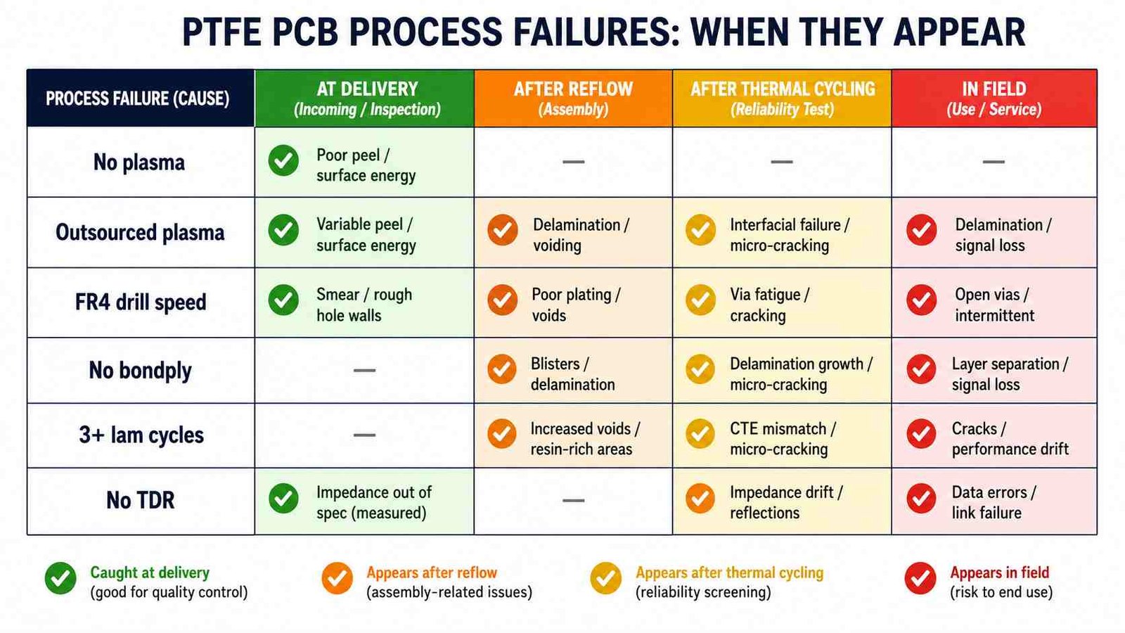
Question-by-Question Explanation
Q1: Is plasma activation in-house?
This is the single most important question. PTFE is chemically inert — copper cannot bond to it without plasma activation. The activation window is 2–4 hours: after that, the surface begins to deactivate. Outsourced plasma means the boards are activated at a third-party facility, packaged, transported, and plated — minimum 4–8 hours later. By the time plating starts, the surface has largely deactivated. See PTFE PCB plasma activation guide for the full chemistry explanation.
Q2: How long between plasma activation and copper plating?
The correct answer is 1–2 hours, same production shift. A factory that cannot give a specific number is not managing this window. A factory that says ‘within the same day’ is almost certainly exceeding the safe window — an 8-hour production shift with plasma at the start and plating at the end is too long.
Q3: What is the RO3003 prototype lead time?
The lead time test is the fastest proxy for plasma capability. RO3003 prototype correctly manufactured: 7–10 working days. The extra 2–3 days vs RO4350B is the plasma activation step within the production sequence. A factory quoting 5–7 days for RO3003 is applying FR4 process to PTFE material. See Rogers PCB prototype China guide for the full lead time breakdown by material.
Q4: Do you stock RO3003 and RT5880?
A factory that stocks these materials has genuine PTFE volume — the capital commitment of maintaining RO3003 and RT5880 inventory (USD 800–1,500/m² for RT5880) signals an actual customer base for these materials, not occasional special orders. A factory that needs to procure material for every order is less likely to have optimised the PTFE process chain.
Q5: What spindle speed do you use for PTFE drilling?
PTFE melts at standard FR4 spindle speed (80,000–120,000 RPM), depositing a smooth PTFE film on the hole wall that blocks plasma activation. Correct PTFE drilling: 40,000–60,000 RPM. A factory that cannot answer this question or says ‘same as FR4’ is applying FR4 drill parameters to PTFE. See PTFE PCB drilling guide for the full parameter comparison.
Q6: Is TDR performed on every production lot?
TDR (time-domain reflectometry) is the standard method for verifying controlled impedance on RF PCB. A supplier performing TDR on every lot catches impedance out-of-spec before shipping. A supplier that only does TDR on request, or never mentions it, is shipping boards without impedance verification — which means you only discover the problem when your RF circuit does not perform.
Q7: What is the maximum lamination cycle count for PTFE?
The correct answer is maximum 2 press cycles. PTFE deforms under repeated heat and pressure — a 3rd cycle causes Dk to shift across the panel and risks delamination at bondply interfaces. A factory that says ‘no limit’ or gives a number higher than 2 is either not manufacturing PTFE or not aware of this constraint. See PTFE PCB lamination guide for the full explanation.
Q8: What bondply do you use for PTFE + FR4 hybrid stackups?
If you are ordering a hybrid Rogers + FR4 stackup, the bondply at the PTFE/FR4 interface must be a Rogers-specific material — Rogers 4450F for RO4350B/RO4003C hybrids, Rogers 2929 for RO3003/RT5880 hybrids. Standard FR4 prepreg at the PTFE interface produces delamination under thermal cycling. A factory that says ‘FR4 prepreg’ or does not know what bondply to use should not be manufacturing hybrid PTFE stackups.
Riching PCB: Answers to All 8 Questions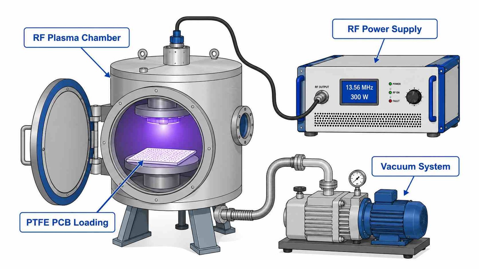
- Q1: Plasma activation in-house — RF plasma chamber on-site, every PTFE order
- Q2: Activation to plating window — 1–2 hours, same production shift
- Q3: RO3003 lead time — 7–10 working days prototype, no material procurement wait
- Q4: Material stock — RO3003, RT5880, RO3006, RO3010, Taconic, F4B in standard inventory
- Q5: PTFE drill speed — 40,000–60,000 RPM, separate drill programs from FR4
- Q6: TDR — every production lot, report available on request
- Q7: Lamination cycles — maximum 2 press cycles for all PTFE materials
- Q8: Bondply — Rogers 4450F for RO4350B hybrids, Rogers 2929 for RO3003/RT5880 hybrids
Conclusion
PTFE PCB failure is a process failure, not a design failure. The 8 questions in this checklist surface the most common process gaps before you place an order: plasma activation in-house and within the 2-hour window, PTFE-specific drill parameters, maximum 2 lamination cycles, correct bondply for hybrid stackups, and TDR on every lot. A supplier that answers all 8 correctly is manufacturing PTFE PCB correctly. A supplier that hesitates on any of the first 3 is a risk. Riching PCB answers all 8. No MOQ. RO3003 and RT5880 in stock. See PTFE PCB manufacturing challenges overview for the complete process guide.