
Metallized Plastic Antenna and PCB Hybrid: Where the Process Stops Working
Metallized plastic antenna PCB hybrids: surface roughness versus skin depth, resin loss, CTE mismatch and the band where additive metallisation stops paying.
Home » 3D Printed Antenna » Metallized Plastic Antenna and PCB Hybrid: Where the Process Stops Working
Table of Contents
Metallised plastic antennas are usually presented as a way to make antennas lighter, cheaper and curved. The useful question is narrower: at which frequency does the process stop paying for itself, and what exactly stops first? That question has arithmetic answers — surface roughness against skin depth, resin loss against length, expansion against the joint, tolerance against guided wavelength — and they point to the same conclusion.
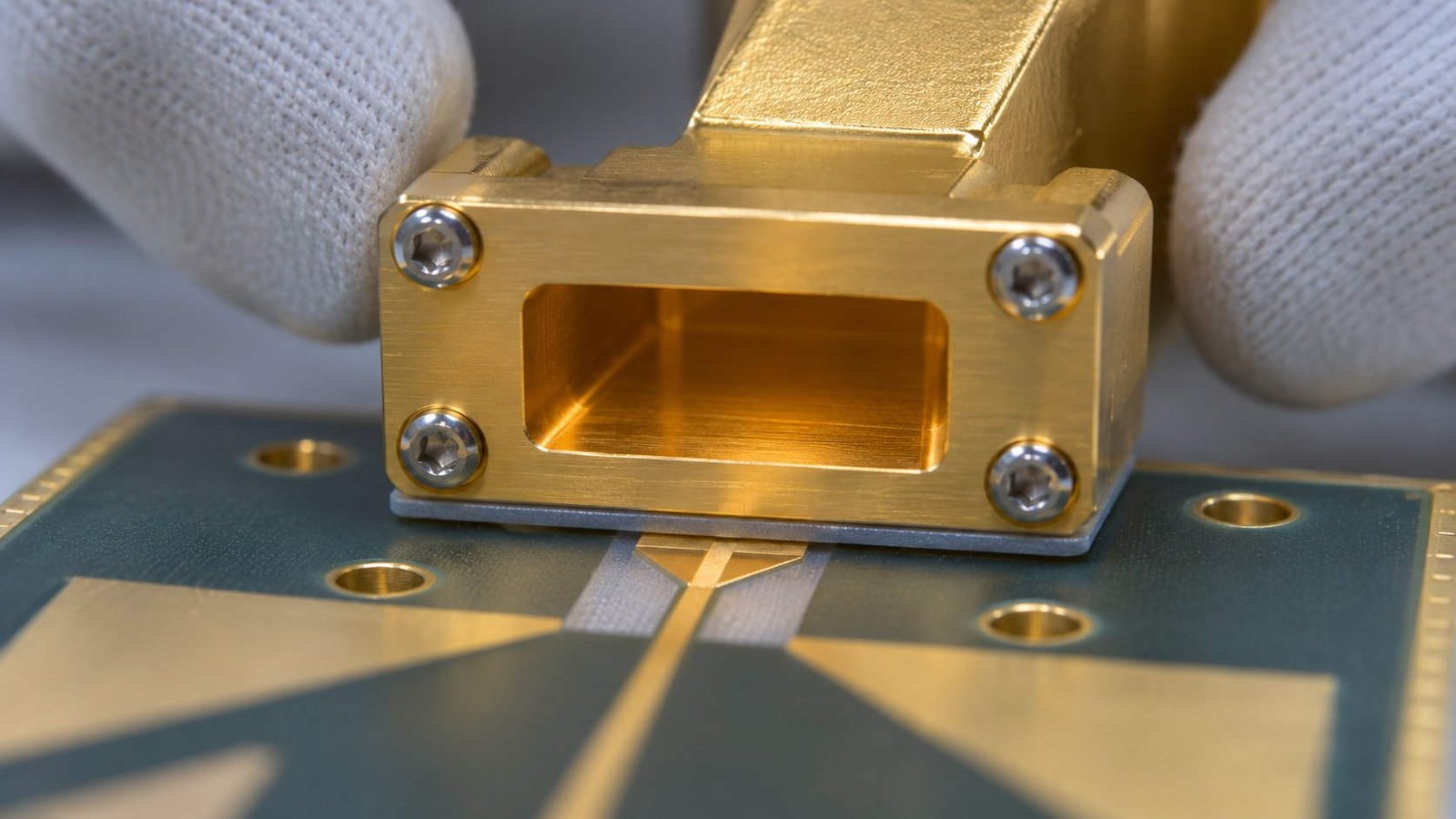
The hybrid that reaches production in automotive radar is not a plastic antenna replacing a PCB antenna. It is a moulded shell that carries the radiating geometry, bolted to a laminate board that carries the feed network and the electronics. The board half is our normal work, and the material choices behind it are set out in our PCB materials for antenna applications section. This page is about the interface and the limits.
1. Two Processes, One Interface
The reason the hybrid exists is not that plastic is cheaper. It is that a 77 GHz radar antenna has to sit behind a curved bumper, and a flat laminate cannot follow that surface while a moulded shell can — and the same shell has nowhere to mount a transceiver.
| Function | Planar PCB antenna | Metallized plastic part | Hybrid (both) |
|---|---|---|---|
| Radiating surface | Etched copper, exact and repeatable | Sprayed or plated shell | Plastic shell carries the radiating geometry |
| Conformal or curved form | Cannot follow a curved bumper | Any shape the mould allows | Curved shell, flat board behind it |
| Feed network and electronics | The reason the board exists | No place to put a transceiver | Board does the RF and DC work |
| Interface count | Zero — it is one part | Zero | One launch per radiator, and it must align |
| Cost at 77 GHz, volume | Low, mature | Low per part, high tooling | Two supply chains to control |
The hybrid exists because neither process covers the whole job: plastic gives the shape, laminate gives the electrical function. Everything difficult about the hybrid sits in the one interface between them.
Read the last row as the actual cost of the approach. A planar antenna has no interface; a hybrid has one per radiator, and every one of them must align to a fraction of a wavelength while the two halves expand at different rates. The interface is not a detail of the design — for practical purposes it is the design.
2. Surface Roughness Against Skin Depth
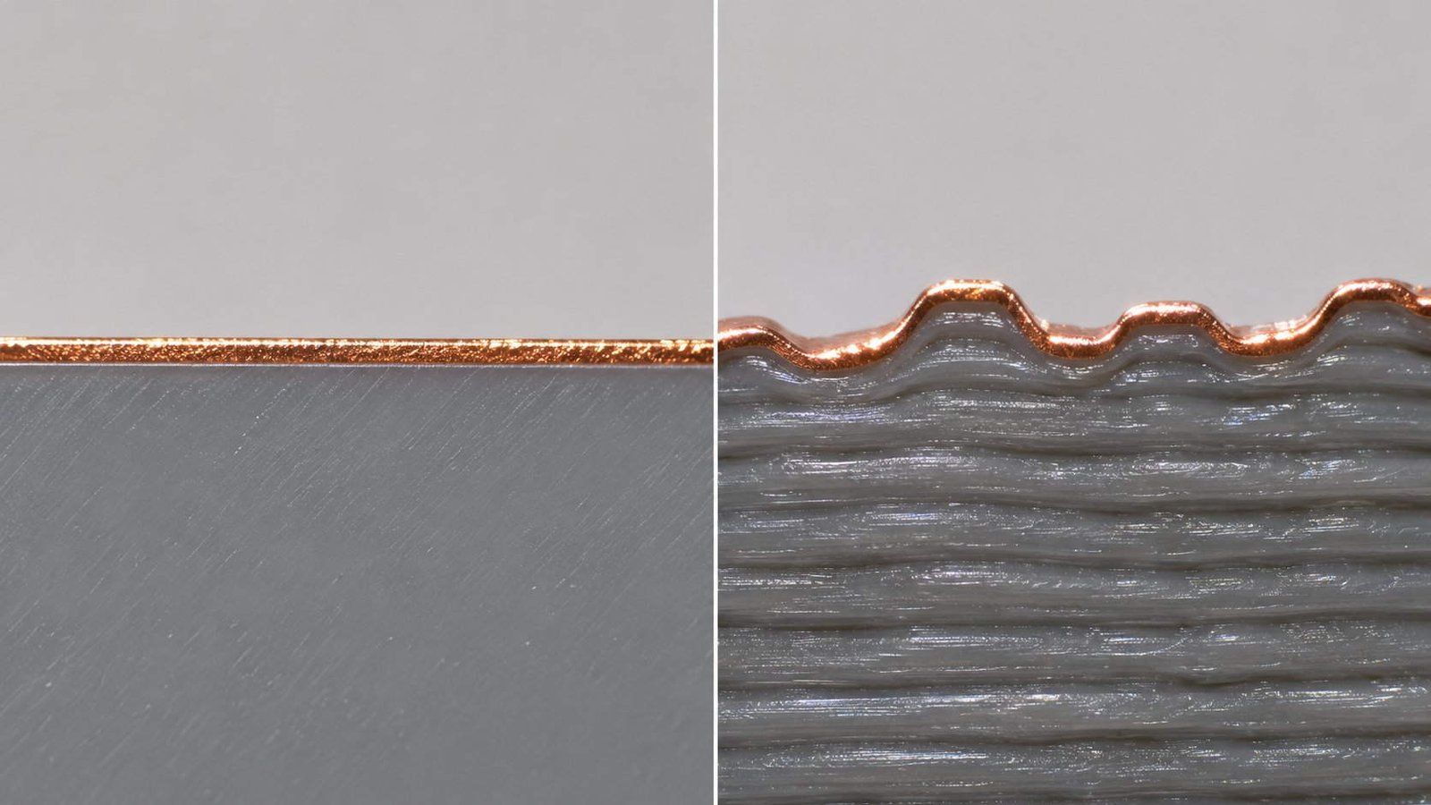
Conductor loss at microwave frequencies depends on how deep the current actually penetrates, and at millimetre waves that depth is small enough to be compared with the texture of a plated plastic surface.
| Process route | Achievable Ra | Ra / δ at 77 GHz (δ = 0.235 µm) | Ra / δ at 950 GHz (δ = 0.067 µm) |
|---|---|---|---|
| Electroplated injection moulding | 0.3 µm | 1.28 | 4.48 |
| SLA print, post-processed, plated | 1.5 µm | 6.38 | 22.4 |
| FDM print, plated as-printed | 8.0 µm | 34.0 | 120 |
The working criterion is Ra ≤ δ. Injection moulding with electroplating sits just outside it at 77 GHz and well outside at 950 GHz. A printed shell that is smooth to the eye is still an order of magnitude too rough for the sub-millimetre band — and plating thickness does not change that, because the copper follows the resin beneath it.
The comparison in the table is the whole argument, and it explains a result that otherwise looks arbitrary: metallised plastic antennas work well at 24 and 77 GHz and become laboratory demonstrations above 300 GHz. Nothing about the metal changed. The surface it was plated onto stopped being smooth relative to the depth the current uses. The finish requirements that follow from this are the same family as those for RF surface finish on laminate, applied to a much rougher substrate.
3. Resin Loss and the Length It Buys
Printed and moulded resins are lossier than microwave laminates by roughly an order of magnitude, and that number is quoted as a disqualification far more often than it deserves.
| Quantity at 77 GHz | Printed resin (Dk 2.90, Df 0.006) | PTFE laminate (Dk 2.20, Df 0.001) |
|---|---|---|
| Dielectric loss | 0.0716 dB/mm | 0.0104 dB/mm |
| Over a 20 mm radiator feed | 1.43 dB | 0.21 dB |
| Over a 50 mm run | 3.58 dB | 0.52 dB |
| Ratio | 6.9× the laminate | Reference |
A factor of 6.9 in dielectric loss sounds disqualifying until you put a length on it. The resin is acceptable across a radiator feed of a couple of centimetres and unacceptable across a corporate network — which is precisely why the hybrid assigns the short paths to plastic and the long ones to laminate.
Put a length on the loss and the division of labour becomes obvious. A radiator feed of two centimetres costs a fraction of a dB in resin; a corporate network of five centimetres costs more than the antenna gain it is feeding. This is why the hybrid gives the short paths to the moulded part and keeps the long ones on laminate — where the loss budget is set by Dk and Df of a material chosen for exactly this reason.
4. The CTE Step at the Joint
Two materials with different expansion coefficients, fastened together and cycled over an automotive temperature range, will move relative to each other. The only question is what absorbs the movement.
| Material pair | CTE (ppm/K) | Expansion over 20 mm, 165 K span | Phase at 77 GHz |
|---|---|---|---|
| Resin shell vs FR-4 / PTFE board | 60 vs 16 | 145.2 µm | 13.4° |
| PTFE shell vs FR-4 board | 28 vs 16 | 39.6 µm | 3.7° |
| Board in-plane, for reference | 16 | — | — |
Over an automotive −40 to +125 °C cycle the interface slides 145.2 µm, and at 77 GHz that is 13.4° of electrical length. A rigid solder bridge across that joint will either crack or drag the board with it. The joint has to be compliant by design, not by hope.
145.2 µm is not a small number. At 77 GHz it is 13.4° of electrical length, which is several times the phase error an antenna calibration would tolerate — and it is also a mechanical shear that a solder fillet of a few tenths of a millimetre cannot absorb for a thousand cycles. The joint has to be compliant, and the electrical consequence of that compliance has to be measured, not assumed. Board-level practice for these assemblies is covered under RF PCB assembly.
5. Tolerance Measured Against the Wavelength
Moulding tolerances are quoted in millimetres and judged against mechanical drawings. The useful judgement is against the wavelength the part is supposed to control.
| Dimension | 77 GHz (WR-10) | 950 GHz (WR-1) |
|---|---|---|
| Free-space wavelength | 3.893 mm | 0.3156 mm |
| Waveguide broad wall | 2.54 mm | 0.254 mm |
| Cut-off frequency, nominal | 59.0 GHz | 590.1 GHz |
| Cut-off with a 0.05 / 0.01 mm short wall | 60.2 GHz (−0.05 mm) | 614.3 GHz (−0.01 mm) |
| Guided wavelength, nominal | — | 0.4027 mm |
| Guided wavelength, short wall | — | 0.4137 mm (+2.7%) |
| Quarter guided wavelength | — | 0.1007 mm |
At 77 GHz a ±0.05 mm moulding tolerance is a routine number. At 950 GHz the same percentage is ±10 µm, the guided wavelength moves 2.7%, and a quarter-wave feature is only 0.101 mm long. Additive processes that hold ±0.05 mm comfortably cannot hold this — the demonstration parts that reach 950 GHz are machined or lapped after printing.
Re-read the 77 GHz column: a ±0.05 mm tolerance moves cut-off by about a gigahertz inside a band that is thirty gigahertz wide, and nobody notices. The identical percentage at 950 GHz moves cut-off by twenty-four gigahertz and the guided wavelength by 2.7%. That is why the frequency ceiling of a printed part is a tolerance statement rather than a materials statement, and why the transition from a moulded horn to a board launch has to be toleranced in the same breath — the alignment side of it is treated in our PCB to waveguide transition guide.
6. The Hybrid RFQ Checklist
Related reading
- antenna OTA and RCS test coupon PCB — far-field distance, mounting repeatability and thermal drift at 77 GHz
- PCB to waveguide transition design — the launch geometry and its alignment tolerance
- RF PCB assembly — joint, process and thermal-cycle practice for RF builds
- automotive radar PCB qualification — PPAP evidence, thermal cycling and the audit trail
- phased array PCB design and manufacturing — element pitch, feed networks and Dk control on the analogue side
Eight lines. On a hybrid assembly, lines 2 and 5 are the ones that decide whether the part works in the field or only on the bench it was measured on.
| # | Item to specify | Why it decides the outcome |
|---|---|---|
| 1 | Which surface carries the radiating geometry | Plastic and laminate cannot both be the reference |
| 2 | Achievable Ra on the metallised surface, with a coupon | Compare it to δ at the top of the band, not to a drawing |
| 3 | Metallisation stack and its adhesion test method | Plating that passes a tape test can still fail 1000 thermal cycles |
| 4 | Resin Dk / Df and moisture uptake | Printed resins absorb water; Df moves with it |
| 5 | Interface geometry and its alignment tolerance | One launch per radiator — plus or minus 0.1 mm is 0.35 dB at 77 GHz |
| 6 | Compliant joint design across the CTE step | 145.2 µm of sliding has to go somewhere |
| 7 | Thermal cycle and the electrical test that follows it | Electrical drift after cycling is the real acceptance |
| 8 | Who owns the tooling and who owns the RF test | Two suppliers, one interface — define the owner |
Lines 2 and 5 are the two that separate a working hybrid from a prototype that measured well once.
The pattern is the same as anywhere else in high-frequency work: the process is not judged by its best sample but by the distribution it can hold, and the interface is not judged by its nominal geometry but by the tolerances on both sides of it. A hybrid that names its surface roughness, its resin data and its joint compliance is a different class of drawing from one that names a material and a shape. The board-side DFM rules that make the laminate half repeatable are in our high-frequency PCB DFM review."
Metallized Plastic Antenna and PCB Hybrid — Frequently Asked Questions
Where additive and moulded metallisation works with laminate, and where surface roughness, resin loss and geometric tolerance stop it: the numbers behind the division of labour.
Why combine a metallized plastic part with a PCB at all?
Because the two processes cover disjoint parts of the job. A 77 GHz automotive radar antenna has to sit behind a curved bumper, and a flat laminate cannot follow that surface; a moulded shell can. But the same shell has nowhere to put a transceiver, a power supply or a feed network, and laminated board does. The hybrid gives the shape to plastic and the electrical function to laminate. The interface between the two is where the design risk concentrates, and the transition itself is a subject in its own right — see our PCB to waveguide transition guide.
How smooth does the plated surface have to be?
The working criterion is that surface roughness should stay at or below the skin depth at the top of the operating band. At 77 GHz the skin depth in copper is 0.235 µm, so an electroplated injection moulding at Ra 0.3 µm sits at 1.28 times that — borderline but usable, and it is what production parts use. At 950 GHz the skin depth falls to 0.067 µm and the same surface is 4.48 times too rough. The important consequence is that plating thicker copper does not help: the metal replicates the resin underneath it.
Can a 3D printed part be used as the radiator?
For a demonstrator, yes, and this is how most published results above 100 GHz are produced. For production, the arithmetic is unforgiving: a printed and post-processed shell lands around Ra 1.5 µm, which is 6.4 times the skin depth at 77 GHz and 22 times at 950 GHz. Printed parts also carry porosity and layer lines that survive plating. The honest statement is that printing is a prototyping route for the geometry and a machining route for the final surface.
What does the resin cost in insertion loss?
At 77 GHz, a printed resin with Dk 2.90 and Df 0.006 dissipates about 0.072 dB/mm, against 0.010 dB/mm for a PTFE laminate — a factor of 6.9. Over a 20 mm radiator feed that is 1.43 dB against 0.21 dB, which is acceptable; over a 50 mm run it becomes 3.58 dB and is not. This single comparison explains the division of labour in a hybrid: short paths to the moulded part, long paths to the board. Material options for the board side are set out in our PCB materials for antenna applications section.
What breaks first over thermal cycling?
The joint, not the plating. The resin shell expands at about 60 ppm/K against 16 ppm/K in-plane for the board, so across a 165 K automotive span a 20 mm interface slides 145.2 µm — 13.4° of electrical length at 77 GHz. If that movement is carried by a rigid solder fillet, the fillet becomes the failure site. Compliant joints, controlled fastener spacing and an electrical test after cycling are what convert the calculation into a qualified part. Assembly and joint practice for these boards is covered in our RF PCB assembly page.
Does the hybrid approach scale to 950 GHz?
As a demonstration, yes — metallised plastic antenna hardware has been shown at that order of frequency. As a production route, the tolerances decide it. At 950 GHz the guided wavelength in WR-1 is 0.403 mm, a quarter-wave feature is 0.1007 mm, and a 0.01 mm deviation on the broad wall moves cut-off from 590 to 614 GHz and the guided wavelength by 2.7%. Printing holds ±50 µm at best. The parts that work above 300 GHz combine printing for the shape with machining or lapping for the critical surface.
Building a hybrid antenna assembly?
Send the radiating geometry, the band and the interface drawing. We will tell you which surface should carry the RF function, what surface finish the band actually requires, and how to size the joint for the CTE step — then build the laminate half and provide the interface data your moulding supplier needs.
Contact Us → WhatsApp: +86 137 6047 3650Request a PCB Quote
Upload your Gerber ZIP file and project requirements. Our engineering team will review your PCB material, stackup, impedance needs, surface finish, and production quantity before quoting.
Please prepare:
- Gerber files in ZIP format
- PCB material or stackup requirements
- Controlled impedance notes if available
- Prototype or batch production quantity