The most common reason a high frequency PCB quotation takes longer than expected — or comes back with questions, holds, or revised pricing — is incomplete submission. Missing the stackup drawing, specifying ‘Rogers PCB’ without the grade, omitting the impedance tolerance, or sending Gerber files without a drill file are the four issues that cause the most delays in our engineering review.
This guide covers exactly what to include when submitting a high frequency PCB quotation request — what each file is, why it matters, and what happens if it is missing. Following this checklist means your order goes from submission to confirmed quotation without back-and-forth.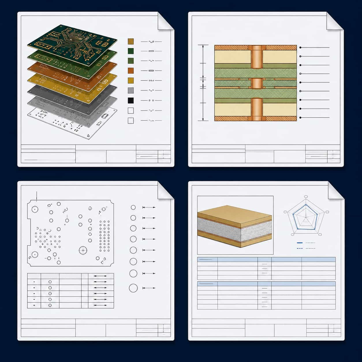
Quick Summary: The Complete File Checklist
Minimum required for any high frequency PCB quotation: Gerber files (all copper layers + solder mask + silkscreen) + NC drill file + complete stackup drawing with material grade, layer sequence, dielectric thickness, and copper weight per layer + controlled impedance requirements if applicable. Without these four elements, a quotation cannot be confirmed — only estimated.
1. Gerber Files — The PCB Design Data
Gerber files are the industry-standard format for PCB layer data. Each layer of the PCB is exported as a separate Gerber file. The complete Gerber package for a high frequency PCB should include:
Required Gerber Layers
- Copper layers: one file per copper layer — top copper, inner layers (numbered), bottom copper
- Solder mask: top and bottom solder mask files
- Silkscreen: top and bottom legend/silkscreen files
- Board outline: mechanical layer defining the exact board dimensions and cutouts
- Paste mask: required if SMT assembly is included; optional for bare board quotation
Gerber Format
- RS-274X (Extended Gerber): the standard format — all modern PCB tools export this
- Gerber X2: newer format with embedded layer type information — also acceptable
- Do not submit: RS-274D (older format without aperture definitions), or native CAD files (Altium .PcbDoc, Eagle .brd, KiCad .kicad_pcb) without first exporting to Gerber
- File naming: clearly label each layer — TOP.gbr, GND.gbr, PWR.gbr, BOT.gbr, etc. — generic names like Layer1.gbr cause confusion and slow DFM review
Common Gerber Submission Mistakes
- Missing the board outline layer: without the outline, the factory cannot confirm board dimensions or panel utilization
- Wrong scale: Gerber exported at wrong units (mm vs inches) produces a board 25.4× the intended size — always confirm units in the export settings
- Missing inner layers: submitting only top and bottom copper for a 4-layer board — inner layers must be included
- Old revision files mixed with new: always submit a clean export from the final revision — label with revision number
How we handle Gerber review: Our engineering team opens every Gerber file before confirming a quotation. We check layer count consistency, board outline completeness, and copper-to-edge clearances. If there is a mismatch between the Gerber layer count and the specified stackup, we flag it before production — not after.
2. NC Drill File — Via and Hole Data
The NC drill file (also called Excellon drill file) tells the factory where every hole is located, what diameter it is, and whether it is plated or non-plated. For high frequency PCB with via fences, thermal via arrays under GaN chips, or blind via structures, the drill file is as important as the copper layers.
What the Drill File Must Include
- All hole coordinates: every through-hole via, component hole, mounting hole, and tooling hole
- Hole diameter: specified for every drill size — use finished hole diameter (after plating), not drill diameter
- Plated vs non-plated: PTH (plated through-hole) and NPTH (non-plated) must be separated — some tools export them as separate files
- Units: confirm mm or inches — the same unit confusion that affects Gerber also affects drill files
For Blind and Buried Via Designs
- Separate drill files for each via stage: blind via layer 1-2 and through-hole require separate drill files
- Via start and stop layers must be specified: ‘blind via from layer 1 to layer 2’ — not just ‘blind via’
- Laser via diameter: for HDI designs with laser blind vias, specify laser via diameter separately from mechanical drill
For blind and buried via design requirements, see Blind and Buried Via Capabilities in High Frequency PCB Manufacturing.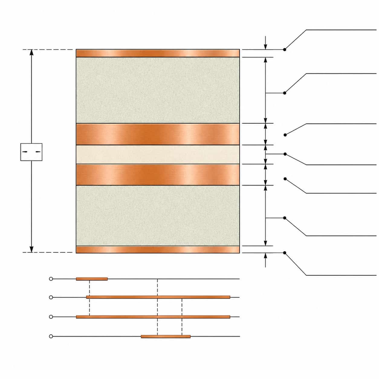
3. Stackup Drawing — The Most Important Document for High Frequency PCB
For standard FR4 PCB, a stackup is sometimes optional — the factory can apply a default stackup for the specified layer count and thickness. For high frequency PCB with Rogers, PTFE, Taconic, or hybrid materials, the stackup drawing is mandatory. Without it, an accurate quotation is impossible.
What the Stackup Drawing Must Specify
- Layer sequence: every layer from top to bottom — copper layers, dielectric layers, and bonding film layers in order
- Material grade for every dielectric layer: Rogers RO4350B, Rogers RO3003, FR4, Rogers RO4450F bondply — each layer specified by grade, not just ‘Rogers’ or ‘high frequency material’
- Dielectric thickness for every layer: in mm, for each dielectric layer between copper layers
- Copper weight for every layer: in oz or µm, for every copper layer
- Total finished board thickness: with tolerance — e.g. 1.6 mm ±0.15 mm
- Copper foil type: standard electrolytic copper (ED) or rolled annealed (RA) — specify if RA is required for flex or fine-line applications
Example: What a Complete 4-Layer Rogers Stackup Looks Like
- Layer 1: Rogers RO4350B, 0.508 mm, 1 oz copper (top signal / RF layer)
- Bonding film: Rogers RO4450F, 0.101 mm
- Layer 2: 1 oz copper (ground plane)
- Core: Rogers RO4350B, 0.508 mm
- Layer 3: 1 oz copper (power plane)
- Bonding film: Rogers RO4450F, 0.101 mm
- Layer 4: Rogers RO4350B, 0.508 mm, 1 oz copper (bottom signal layer)
- Total thickness: approximately 1.57 mm
Common Stackup Specification Mistakes
- Specifying ‘Rogers PCB’ without the grade: RO4350B, RO4003C, RO3003, and RT5880 have completely different properties and prices — the grade must be specified
- No bonding film specified for hybrid stackups: Rogers RO4350B + FR4 requires Rogers RO4450F bondply — standard FR4 prepreg at the interface is a manufacturing error
- Dielectric thickness not specified: saying ‘4-layer, 1.6 mm total’ without dielectric layer thicknesses means the factory must assume — assumptions may not match your impedance calculation
- Copper weight missing: affects impedance calculation, etching process, and minimum line width capability
- Total thickness without tolerance: specify both target and tolerance — e.g. 1.6 mm ±0.15 mm
For Rogers material selection guidance to fill in your stackup, see Rogers PCB Material Selection Guide. For hybrid FR4 + Rogers stackup design, see Mixed Laminate High Frequency PCB: How FR4 and Rogers Are Combined in Production.
4. Controlled Impedance Requirements
Controlled impedance is a core requirement for high frequency PCB. If your design has impedance-controlled traces — 50Ω microstrip, 100Ω differential pair, coplanar waveguide — this must be specified in the quotation request. Without it, the factory cannot confirm whether the specified stackup achieves the required impedance.
What to Specify for Controlled Impedance
- Target impedance value: e.g. 50Ω single-ended, 100Ω differential
- Impedance tolerance: ±10% standard, ±8% advanced — specify which is acceptable
- Which layer: which copper layer carries the impedance-controlled trace
- Trace width reference: the trace width on the Gerber that should achieve the target impedance — the factory will verify this in DFM
- Transmission line structure: microstrip, stripline, coplanar waveguide, or grounded coplanar waveguide
What Happens During Our DFM Review
When we receive a high frequency PCB quotation with impedance requirements, our engineering team recalculates the impedance using our confirmed production Dk value from the material certificate — not the nominal datasheet value. If the calculation shows the specified trace width does not achieve the target impedance within tolerance, we report this before production with the corrected trace width.
- We use confirmed production Dk, not nominal — a 2% Dk variation produces a ~1% impedance shift
- We include bonding film Dk contribution for hybrid stackups — often overlooked in customer calculations
- We specify impedance coupon placement on the panel edge — and provide the coupon design
- TDR verification: every production lot — coupon measurement records available on request
For controlled impedance background, see Why Controlled Impedance Matters in RF PCB Manufacturing.
5. PCB Specifications — What Else to Include
Beyond the files and stackup, the following specification parameters are needed for a complete high frequency PCB quotation:
Board Dimensions and Panel
- Finished board dimensions: length × width in mm
- Board quantity: number of individual boards or panels
- Panelization: if boards should be panelized (v-score, tab-routed, or solid panel) — specify preferred panel layout or leave to factory recommendation
- Board outline tolerance: standard ±0.15 mm, tight ±0.1 mm
Surface Finish
- ENIG: most common for high frequency PCB — specify nickel thickness (standard 120–300 µin) and gold thickness (standard 1–3 µin)
- ENEPIG: for aerospace/defense programs or wire-bonded components — eliminates black pad risk
- Immersion Silver: for Ka-band and above where nickel layer RF loss matters
- Immersion Tin or OSP: generally not recommended for high frequency PCB — poor shelf life and uneven surface
For surface finish selection guidance, see ENIG vs ENEPIG vs Immersion Silver for High Frequency PCB.
Quality Standard
- IPC Class: specify Class 2 (commercial) or Class 3 (aerospace/defense/high reliability)
- IPC Class 3 requires: 25 µm average PTH copper plating, no annular ring breakout, 5% maximum void, 100% electrical test, microsection FAI
- Applicable standards: IPC-6012 (rigid PCB), IPC-6015 (microwave PCB), MIL-PRF-31032 (military) — specify if applicable
Special Requirements
- Via fill: copper-filled, resin-filled, or standard open via — specify for thermal vias under GaN chips or via-in-pad designs
- Back drilling: specify stub length target (e.g. ≤10 mil) and depth tolerance (±0.1 mm) for back-drilled via designs
- Impedance test coupon: confirm coupon placement on panel edge — required for TDR verification
- Traceability: Rogers-certified material certificates required for aerospace/defense programs — specify lot number retention requirement
- Conformal coating: specify type and coverage if required — acrylic, polyurethane, or silicone

What Happens After You Submit Files: Our Engineering Review Process
As a direct high frequency PCB factory, every quotation submission goes through an engineering review before the quotation is confirmed. This is not a sales team review — it is a process engineering review by the team that will build the board.
What We Check in DFM Review
- Stackup feasibility: can the specified layer count, material, and dielectric thickness be built within our confirmed process limits?
- Impedance calculation: we recalculate using production Dk — if the specified trace width does not achieve the target impedance, we report the correction
- Via aspect ratio: every via checked against our aspect ratio limit for the specified material and board thickness
- Minimum annular ring: confirmed for IPC Class 2 or Class 3 based on specified quality standard
- PTFE process compatibility: for Rogers RO3003, RT5880, Taconic, or F4B — plasma activation process confirmed, lamination cycle count verified
- Bonding film availability: Rogers RO4450F for RO4350B hybrids, Rogers 2929 for PTFE hybrids — confirmed in inventory
- Material availability: specified Rogers, Taconic, or F4B grade and thickness confirmed in stock
- Lead time: confirmed based on actual factory schedule, not estimated
What You Receive With the Quotation
- Confirmed stackup with production Dk values used for impedance calculation
- DFM feedback on any issues that require design changes before production
- Confirmed impedance tolerance achievable for the specific design
- Material availability confirmation
- Lead time based on actual factory capacity
- Impedance coupon design recommendation
Direct factory advantage: When you submit files to a direct factory, the DFM review is done by production engineers — not by a sales team passing files to a third party. For high frequency PCB with PTFE materials, blind via structures, or tight impedance tolerances, this difference matters. A problem caught in DFM costs nothing to fix. The same problem found after production costs the full board price and the lead time.
Complete Submission Checklist
Use this checklist before submitting a high frequency PCB quotation request:
Files
- ☐ Gerber files — all copper layers, solder mask, silkscreen, board outline
- ☐ NC drill file — all hole sizes, PTH and NPTH separated, correct units
- ☐ Separate drill files for blind/buried via stages if applicable
- ☐ Assembly drawing or BOM if PCBA quotation is included
Stackup
- ☐ Material grade specified for every layer — Rogers grade, not just ‘Rogers PCB’
- ☐ Dielectric thickness for every layer in mm
- ☐ Copper weight for every layer in oz or µm
- ☐ Bonding film specified for hybrid stackups
- ☐ Total finished board thickness with tolerance
Specifications
- ☐ Controlled impedance target value and tolerance if applicable
- ☐ Transmission line structure if non-standard
- ☐ Board dimensions and quantity
- ☐ Surface finish — ENIG, ENEPIG, immersion silver
- ☐ IPC Class — 2 or 3
- ☐ Via fill requirement if applicable
- ☐ Back drill specification if applicable
- ☐ Material certification requirement — Rogers lot certificate for aerospace/defense
- ☐ Applicable standards — IPC-6012, IPC-6015, MIL-PRF-31032
- ☐ Delivery requirement — standard or expedite
Contact Information
- ☐ Project name or PO reference
- ☐ Application type — helps engineering team confirm correct material recommendation
- ☐ Operating frequency range — needed if material has not been finalized
- ☐ Reply-to contact for DFM questions
The Most Common Causes of Quotation Delays
These are the issues that cause engineering holds in high frequency PCB quotation — in order of frequency:
- No stackup drawing. Most common cause of delay. Without a stackup, the factory must either assume or ask. Assumptions may not match your impedance calculation.
- Rogers grade not specified. ‘Rogers PCB’ or ‘high frequency material’ is not a specification. RO4350B, RO4003C, RO3003, and RT5880 have different prices, processes, and lead times.
- Missing drill file. Gerber files without a drill file are incomplete. Every hole must be specified.
- No impedance specification. If the design has RF traces and no impedance specification is provided, the factory cannot confirm whether the stackup achieves the required impedance.
- Inconsistent layer count. Gerber shows 6 copper layers but stackup specifies 4. This requires clarification before production.
- Wrong copper weight on Gerber vs stackup. Impedance calculation is sensitive to copper thickness — inconsistency requires clarification.
- PTFE material specified but process requirements not addressed. Plasma activation, bonding film, and lamination cycle limits must be confirmed before production starts.

Application-Specific Quotation Notes
Aerospace and Defense High Frequency PCB
- Rogers-certified material certificates with lot numbers: specify retention period — typically 20–30 years for defense programs
- IPC Class 3 mandatory: specify on fabrication drawing and quotation request
- Applicable standards: MIL-PRF-31032 for US military programs
- Conformal coating: specify type, thickness, and coverage verification method
- Traceability: specify serialization requirement if applicable
See: High Frequency PCB for Aerospace and Defense
Ka-Band and mmWave PCB
- Rogers RO3003 or RT5880: specify substrate thickness — 0.127 mm or 0.254 mm for Ka-band
- Minimum line width: confirm with factory that 2.5 mil line width is achievable on the specified substrate — not all factories can achieve this on PTFE
- PTFE process confirmation: ask the factory to confirm plasma activation capability before submitting
- Antenna element dimensions: provide if available — helps DFM review confirm dimensional tolerance feasibility
See: Rogers PCB Material Selection Guide
Heavy Copper RF PCB
- Copper weight specified per layer: 2 oz, 3 oz, 4 oz, or heavier — do not leave as default
- Minimum line width compliance: confirm that all traces on heavy copper layers meet the minimum width for the specified copper weight
- Via aspect ratio: heavy copper boards are thicker — verify aspect ratio against factory limit
See: Heavy Copper High Frequency PCB
Multilayer High Frequency PCB
- Layer count and complete stackup: essential — default assumptions do not apply for Rogers multilayer
- Lamination cycle count: for PTFE multilayer, confirm total press cycles needed — maximum 2 for PTFE
- Blind via stage sequence: specify which layers each blind via stage connects
See: Multilayer High Frequency PCB: Layer Count, Stackup and Manufacturing Limits
How to Submit Files to Riching PCB
As a direct high frequency PCB factory, we accept quotation submissions by email with all files attached in a ZIP archive. Our engineering team reviews every submission before confirming the quotation.
- File format: ZIP archive containing all Gerber files, drill file, and stackup drawing
- Stackup: PDF or Excel — clearly showing every layer with material, thickness, and copper weight
- Additional specs: include in the email body or as a separate PDF
- Response time: standard DFM review and quotation within 24–48 business hours for most designs; complex PTFE or multilayer designs may require an additional day
- DFM feedback: if issues are found, we respond with specific technical questions or recommendations before confirming the quote — not after production begins
Direct factory note: We are a manufacturing factory, not a trading company. When you email your files, the engineering team that reviews them is the same team that builds the boards. Questions about PTFE activation, bonding film selection, impedance calculation, or via aspect ratio go directly to the engineers who handle these decisions — not through a sales intermediary.
Conclusion
Getting a high frequency PCB quotation right the first time requires four things: complete Gerber files with a proper board outline, an NC drill file, a complete stackup drawing with Rogers material grade specified for every layer, and controlled impedance requirements if applicable. These four elements allow a direct factory to confirm feasibility, calculate impedance using production Dk values, and provide an accurate quotation without engineering holds.
As a direct high frequency PCB manufacturer with Rogers, Taconic, PTFE, and F4B production capability in our own factory, we review every submission with our engineering team before quoting. Submit your files using the checklist above and receive a DFM-reviewed quotation from the factory that will build your board.