
Antenna Module PCB Assembly: RO4350B/PTFE Substrates, Lamination and QC
Antenna module PCB assembly: substrate choice and material verification, surface rules on the radiating side, lamination and warp control, ground fencing around elements, PIM control and the QC plan behind a finished radiating module.
Home » Antenna PCB » Antenna Module PCB Assembly: RO4350B/PTFE Substrates, Lamination and QC
Table of Contents
Antenna module PCB assembly is the process chain that turns a bare high-frequency laminate panel into a finished, tested radiating module: substrate selection and material verification, lamination of the antenna panel to the required thickness and flatness, the mask and surface-finish decisions on the radiating side, SMT and connector assembly, and RF test before the module ships.
It is not the same task as general PCB assembly. The radiating element is normally left without solder mask, the acceptance criteria are electrical — return loss, gain and passive intermodulation — and the process steps that decide whether the module works are the ones that happen before any component is placed. This guide covers the five stages in that order, with the numbers each one has to hold, for modules from roughly 400 MHz up to 77 GHz.
1. What an Antenna Module Is, and Why Its Assembly Differs
An antenna module is a board whose primary function is to radiate or receive. Everything else on it — the feed network, the control logic, the power section — exists to serve that function. That single fact sets the priorities for the whole assembly chain: the radiating surface cannot be processed like the rest of the board, and the checks that decide pass or fail are made with a network analyser rather than with an AOI camera.
The five module types below cover most production work, and each one shifts the emphasis to a different part of the process. The right-hand column is the part of the assembly that carries the design risk.
| Antenna module type | Typical substrate and dielectric thickness | What the assembly has to protect |
|---|---|---|
| Single / dual patch module 2.4–6 GHz, Wi-Fi, GNSS, IoT gateways | Hydrocarbon laminate, 0.508–1.524 mm | The radiating element stays mask-free, so the finish and the element geometry set the resonant frequency. |
| RF front-end module Sub-6 GHz, paired with digital control | 0.254–0.508 mm RF laminate, often on an FR-4 control board | The feed line impedance and the return path under the RF section, not the antenna pattern. |
| Phased array / array panel 10–40 GHz, radar, SATCOM, 5G mmWave | PTFE composite, 0.127–0.254 mm | Phase and amplitude match across elements, which depends on Dk uniformity and on thickness control across the whole panel. |
| 77 GHz radar antenna module Automotive radar | PTFE composite, 0.127 mm | Panel flatness and thickness tolerance, because the element dimensions are a fraction of a millimetre at this band. |
| High-Dk compact module Size-constrained handheld and wearable | Ceramic-filled laminate, 0.508–1.524 mm | Element dimensional tolerance, since a high Dk shrinks the element and makes a fixed etch tolerance a larger share of it. |
2. Substrate Choice for Antenna Modules
The laminate decision for an antenna module rests on three properties, in this order: dielectric constant and its tolerance, dissipation factor at the operating band, and the dielectric thicknesses the material is actually available in. Mechanical and thermal properties matter, but they are usually satisfied by more than one option.
| Laminate family | Dk @ 10 GHz | Df @ 10 GHz | Standard dielectric thicknesses | What it is specified for |
|---|---|---|---|---|
| Hydrocarbon, RO4350B-class | 3.48 ±0.05 | 0.0037 | 0.168–1.524 mm | Antenna modules that also carry digital control and power, and boards that go through standard multilayer processes. |
| PTFE composite, RO3003-class | 3.00 ±0.04 | 0.0010 | 0.127–1.524 mm | Array panels and mmWave modules where insertion loss and phase stability dominate the budget. |
| PTFE glass-microfiber, RT/duroid 5880-class | 2.20 ±0.02 | 0.0009 | 0.127–3.175 mm | Wideband and millimetre-wave antennas where the lowest available loss is required. |
| Ceramic-filled laminate | 6–10 depending on grade | 0.0020–0.0035 | 0.254–1.524 mm | Compact elements and size-constrained modules, where a shorter guided wavelength is the design lever. |
Typical datasheet values, listed as facts for module planning. Each family is specified for the job it does — the table does not rank them. Always design against the datasheet of the exact grade and lot you order.
Why Dk tolerance carries more weight here than on a general RF board. A patch element resonates at a frequency that scales as one over the square root of Dk. On a 3.48 Dk laminate, a tolerance of ±0.05 corresponds to a frequency shift of roughly ±0.7 %, which is about ±72 MHz at 10 GHz. A single patch on a thicker dielectric has a bandwidth of a few percent, so that shift is manageable — but on a narrowband module, or on an array where every element has to stay on the same frequency, it consumes a real share of the budget.
Why thickness availability matters as much as the datasheet. The element size you get is set by the guided wavelength, which is the free-space wavelength divided by the square root of Dk and multiplied by the thickness-dependent effective value. Choosing a material whose useful gauges do not include the thickness your design needs forces a redesign of the element, not a re-quote. We list the standard gauges in the table above for exactly that reason.
3. Surface Rules on the Radiating Side
This is where an antenna module stops behaving like a normal RF board. Solder mask is a dielectric layer, and on a radiating element it is an uncontrolled one. The decisions in this section are usually made once, in the fabrication drawing, and then either held for the life of the product or lost at the first re-CAM.
| Surface item | Practice on an antenna module | Why |
|---|---|---|
| Radiating element | No solder mask | LPI solder mask has a dielectric constant around 3.5–4.0. A 15–25 µm layer over the element lowers the resonant frequency and adds loss, and its thickness varies over the copper edges. |
| Element surface finish | Immersion silver, or ENIG where the assembly sequence requires it | Leaving the element bare means the copper has to be finished, or it oxidises and cannot be soldered or wire-bonded later. |
| Feed line away from the transition | Solder mask allowed | The field is concentrated at the element and the launch; a mask layer over a 50 Ω line further back shifts impedance by a small, measurable amount that can be simulated. |
| Connector pad | Hard gold or immersion silver | The launch sees the highest current density on the module, and repeated mating erodes plating. |
| Element copper weight | 0.5–1 oz (17–35 µm) | Thinner copper holds finer element gaps; thicker copper reduces conductor loss on the feed network. |
| Mask keep-out | Called out on the fabrication drawing, not left to the factory default | A mask keep-out that is described only in an email tends to disappear when the panel is re-CAMed. |
The mask decision and the finish decision are one decision. Leaving the element mask-free means the copper is exposed, so it has to be finished or it will oxidise. Immersion silver gives the lowest loss and the best PIM behaviour; ENIG is chosen when the element also has to survive a soldering or bonding step elsewhere on the panel. Whichever finish is selected, it has to cover the element uniformly — an uneven finish over a patch changes the effective conductor loss across the array.
Etch tolerance is the second half of the story. A ±20 µm etch tolerance on a 10 GHz element that is a few millimetres across is a fraction of a percent, which is acceptable. On a 30 GHz element the same tolerance is several times larger as a share of the dimension, and on a high-Dk compact module it is larger again. If the band is high enough, the drawing has to state the element tolerance you will accept rather than leaving it to the standard etch class.
4. Lamination: Warp, Thickness and Cycle Limits
Lamination is the stage that decides whether the module can be assembled at all. An antenna panel is usually a large, thin, low-layer-count construction, which is the geometry most sensitive to press behaviour. Six requirements carry almost all of the risk.
| Process step | Requirement for antenna panels | Failure mode if it is missed |
|---|---|---|
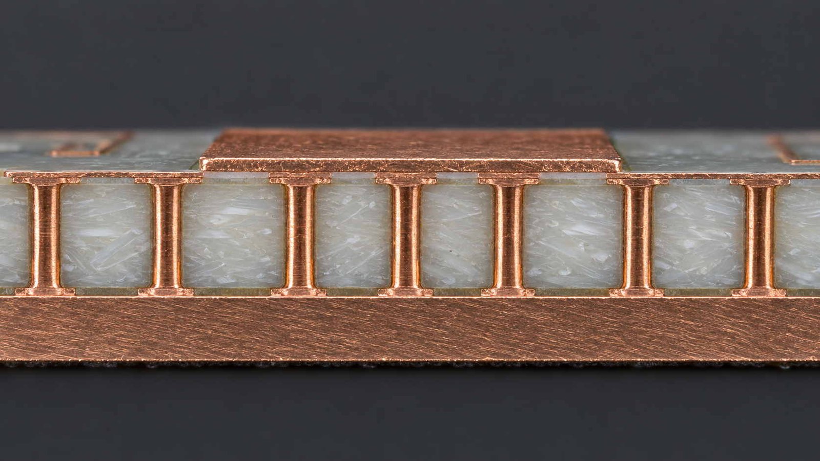
| Bonding layer | PTFE-based bondply for PTFE panels; hydrocarbon prepreg for hydrocarbon panels | A mismatched bond line inside the antenna field changes the effective Dk and can show up as a shifted resonance. |
| Surface preparation | Plasma activation before lamination and a validated desmear after drilling on PTFE | Untreated PTFE bonds poorly; the panel passes first article and delaminates after thermal cycling. |
| Press cycle budget | PTFE composites are normally limited to two lamination cycles | Each extra press stacks thickness error and registration error, and increases the risk of resin starvation at the panel edge. |
| Build symmetry | Symmetric construction about the centre line | An unbalanced build warps, and a warped array panel loses element-to-element phase match. |
| Flatness | Held to roughly 0.5 % of the panel diagonal, or the flatness your SMT line can accept | Flatness outside spec shows up as placement offsets and as inconsistent connector seating. |
| Dielectric thickness | Held on the antenna dielectric layer specifically, not only on the finished board | A thickness error changes the guided wavelength, so the elements and the feed network both detune. |
Never re-press a warped antenna panel to fix flatness. PTFE-based composites are normally limited to two lamination cycles, and each additional press adds thickness and registration error on top of the warp. Fix the build symmetry and the press recipe instead.
The process side of PTFE bonding — plasma activation before lamination, bondply selection and the two-cycle limit on re-pressing — is covered in more depth in our guide to PTFE PCB lamination.
5. Drilling, Plating and the Ground Fence Around Elements
Drilling on an antenna panel is not difficult in terms of aspect ratio — thin dielectrics make that easy — but it is unforgiving about placement and about plating quality inside PTFE. The ground fence around each element group is the single feature most likely to be under-specified on the drawing.
| Feature | Rule for an antenna panel | Reason |
|---|---|---|
| Ground via fence spacing | λ/10 at the highest operating frequency | Keeps the ground reference continuous and suppresses surface-wave leakage between element groups. |
| Fence continuity | No gap larger than the fence pitch, including at corners and around the feed entry | A single wide gap behaves as a slot radiator and couples into the pattern. |
| Vias inside the radiating aperture | Not permitted unless they are intentional shorting pins in the design | Vias through an element area perturb the current distribution and shift resonance unpredictably. |
| Plated through holes in PTFE | Plasma desmear plus a validated plating recipe, verified by microsection | PTFE smears during drilling; without desmear the plating adhesion fails at temperature cycling. |
| Aspect ratio | Typically 8:1 or better on antenna panels | Thin dielectrics make tight aspect ratios easy, but the plating thickness has to stay uniform through the barrel. |
| Via hole tolerance | Drill-to-pad target keeps at least 0.15 mm annular ring after etch | Thin PTFE panels etch aggressively, and a marginal annular ring breaks out on the second press. |
A note on placement discipline. The fence has to be modelled in the layout, not added during CAM. A fence that is inserted at the fabrication stage is placed at the nearest legal pitch rather than at the pitch the design assumed, and on an array the resulting difference between element groups is what shows up as asymmetry in the pattern.
6. SMT, Connectors and PIM Control
Once the panel is laminated and the mask keep-out has survived to production, assembly becomes the stage where an electrically acceptable board can still become an unacceptable module. The items below are the ones that show up in failure analysis, not in incoming inspection.
| Assembly item | Practice | Why it matters on an antenna module |
|---|---|---|
| Connector mounting | Press-fit or edge launch with controlled press force; no rework on the launch itself | The launch sets return loss. Reworked or over-pressed launches are the most common source of a VSWR failure that the bare board passes. |
| Shield can attach | Pre-tinned frame, seam or spot soldered, no flux residue trapped under the can | Residue under a shield changes the local dielectric loading and can create a low-level contact that degrades PIM. |
| RF and control device attach | SAC305 reflow, ground and thermal pad voiding held below 25 % of pad area | Voiding under a ground pad raises RF ground inductance, which shows up as gain and isolation loss rather than as a visible defect. |
| Cleaning | Ionic contamination held below 1.56 µg NaCl/cm² equivalent per J-STD-001 | Uncleaned flux residue on a radiating surface is both a loss and a long-term corrosion risk. |
| Coating | Conformal coating excluded from the radiating area and from connector threads | Coating over an element adds an uncontrolled dielectric layer; coating on a thread changes the connector interface. |
| PIM control | Non-magnetic finishes, controlled nickel thickness, specified torque, clean joints | Passive intermodulation in a base station antenna module is a system-level failure, and it is decided by surface finish and by joint quality, not by the laminate. |
PIM deserves its own sentence. Passive intermodulation is generated by non-linear junctions: oxide layers, loose contacts, magnetic plating such as nickel, and flux residue in a joint. On a transmit antenna module it is a system-level failure that appears only at high power, so it is controlled through finish selection, plating thickness, torque specification and cleanliness — none of which are visible on a finished board. If the module transmits, the PIM target and its test condition belong on the drawing.
Where the scope includes component placement and connector mounting rather than bare board fabrication, the sequence and the file set are described in our page on RF PCB assembly.

7. QC and Test Plan for Antenna Modules
An antenna module has two independent acceptance paths: the fabrication checks that prove the laminate and the copper are what the drawing asked for, and the electrical checks that prove the module radiates as designed. A test plan that only does the first one passes boards that fail in the field.
| Check | What is measured | What it catches |
|---|---|---|
| Incoming material | Dk and thickness verified on the delivered lot (coupon or supplier certificate) | A grade or lot substitution that would detune every element on the panel. |
| Panel thickness and flatness | Dielectric thickness on the antenna layer, overall thickness, flatness across the panel | Thickness and warp problems before SMT, when they are still cheap to fix. |
| Impedance coupon | TDR on feed-line coupons, typically ±5 % of the target | Feed-network impedance that drifted with etch or with the press cycle. |
| Microsection | Plating thickness, dielectric thickness, via walls, resin fill | Smear, thin plating and delamination that electrical test cannot see. |
| X-ray | Ground and thermal pad voiding, held below 25 % of pad area | Voids that raise ground inductance under RF and power devices. |
| AOI / SPI | Placement, solder volume, missing or rotated devices | Assembly defects on the RF front end of the module. |
| VNA test | S11 / VSWR on each module or on a defined sample, typically VSWR < 1.5:1 over the band | A bad launch, a detuned element or a shield contact problem. |
| Gain and pattern | Anechoic chamber measurement on the first article and on change points | Pattern distortion that a single-port VSWR test cannot detect. |
| PIM test | Two-tone test on sample base station modules, commonly targeting −150 dBc | Finish and joint problems that only appear at high transmit power. |
| Thermal cycling | −55 °C to +125 °C per the applicable specification, with RF test before and after | Delamination and plating failures that a room-temperature test misses. |
| Traceability | Panel, lot, material batch and test data recorded per module | The ability to narrow a field failure to a material lot instead of a whole shipment. |
What to apply to every unit and what to sample. Coupon impedance, AOI and X-ray are per-panel or per-lot checks. VNA return loss is normally applied to every module, because it is fast and it catches launch and assembly problems. Chamber gain and pattern measurement, PIM and thermal cycling are first-article and change-point checks: they are expensive, they are slow, and repeating them on every unit adds cost without adding information once the process is stable.
The general framework for the fabrication-side checks — coupon design, IPC Class 2 versus Class 3 scope and batch traceability — is set out in our guide to RF PCB quality control.
8. What to Send With an Antenna Module RFQ
An antenna module quote turns on details that a general PCB quote does not need. The mask keep-out, the element tolerance, the finish in each area and the test coverage all change the price, and none of them can be inferred from a board outline and a material name. Send these together:
| Item to send | Detail the factory needs |
|---|---|
| Stackup | Layer order with the material and dielectric thickness for every layer, including the antenna dielectric. |
| Material and Dk tolerance | Grade plus tolerance and test frequency — e.g. 3.48 ±0.05 at 10 GHz, not only the trade name. |
| Mask keep-out drawing | The radiating area and any feed-line sections that must stay mask-free. |
| Element and feed geometry | Element dimensions with the etch tolerance you will accept, and the feed network type. |
| Band and VSWR target | Operating band edges and the VSWR or return loss the module must meet. |
| Finish callout | Which areas get which finish, including the connector pads. |
| Connector type and mounting | SMA, 2.92 mm, press-fit pin or edge launch, and the mounting method. |
| Assembly scope | Bare board only, or board plus SMT, connectors and shield cans. |
| PIM target | If the module is a transmit antenna, state the PIM requirement and the test condition. |
| Test coverage | Coupon impedance test, 100 % VNA test or sampled, chamber measurement, thermal cycling. |
| Flatness requirement | The flatness your placement line can accept, so the factory can hold it at lamination. |
| Quantity and build type | Prototype, pilot or production, and the expected repeat volume. |
If the module is an array, send the element pitch and the panel layout as well. The pitch decides how much material is consumed per module and whether the panel can be stepped efficiently, and it is usually the largest single lever on the unit price. The antenna dielectric and stackup options are set out on our antenna PCB manufacturing page, and the array-specific tolerances are covered in our phased array PCB guide.
If the design is still open on the laminate, say so in the request. Agreeing the material and the dielectric thickness before the quote is faster than changing them afterwards, and it keeps the element dimensions valid. The substrate side of that decision is set out in our guide to RO4350B PCB, which is the grade most sub-6 GHz antenna modules are built on.
Antenna Module PCB Assembly — Frequently Asked Questions
Direct answers to the questions engineers and buyers ask before releasing an antenna module for assembly.
What is antenna module PCB assembly?
Antenna module PCB assembly is the process chain that turns a bare high-frequency laminate panel into a finished, tested radiating module. It covers substrate selection and material verification, lamination of the antenna panel to the required thickness and flatness, the mask and surface-finish decisions on the radiating side, SMT and connector assembly, and RF test before the module ships. It differs from general PCB assembly because the radiating surface stays mask-free and because the acceptance criteria are electrical — VSWR, gain and PIM — rather than only solder-joint quality.
Should the radiating element of an antenna module have solder mask on it?
No. Production antenna modules normally leave the radiating element mask-free. LPI solder mask has a dielectric constant around 3.5 to 4.0, and a 15 to 25 µm layer over an element lowers the resonant frequency and adds loss. Because mask thickness also varies over copper edges, a masked element carries an uncertainty that is difficult to simulate accurately. The element is instead protected by a finished surface such as immersion silver, specified through a mask keep-out on the fabrication drawing.
Which dielectric thickness is used for a patch antenna module?
It depends on the band and on the bandwidth required. A patch on a 3.48 Dk laminate is commonly built on 0.508 mm for narrowband modules around 5 to 6 GHz and on 0.762 mm for 2.4 GHz designs, because a thicker dielectric widens the patch bandwidth at the cost of a larger element. Array panels that operate from 10 GHz upward typically use 0.127 mm to 0.254 mm PTFE composite, where a thin, tightly controlled dielectric keeps the guided wavelength short and the elements small.
Can an antenna panel be re-pressed if it warps after lamination?
Normally not more than the material allows. PTFE-based composites are commonly limited to two lamination cycles, and every additional press stacks thickness error and layer-to-layer registration error. On an array panel that means element positions and the feed network both move, which cannot be recovered by trimming. A warped panel is a build problem: it is resolved by making the construction symmetric and by correcting the press recipe, not by pressing the same panel again.
Sending an antenna module to production?
Send us the stackup, the mask keep-out drawing and the band you need covered. Our engineers review the antenna dielectric, the lamination sequence that holds the panel flat, and the test plan — then quote fabrication, or fabrication plus assembly, on the exact laminate grade you specify.
Contact Us → WhatsApp: +86 137 6047 3650Request a PCB Quote
Upload your Gerber ZIP file and project requirements. Our engineering team will review your PCB material, stackup, impedance needs, surface finish, and production quantity before quoting.
Please prepare:
- Gerber files in ZIP format
- PCB material or stackup requirements
- Controlled impedance notes if available
- Prototype or batch production quantity