
Arlon AD255C PCB: Antenna-Grade PTFE Laminate for Base Station and Telematics Antennas
Arlon AD255C PCB: antenna-grade PTFE laminate data in real numbers, how the woven glass and ceramic fill behave in fabrication, and the antenna use cases the AD Series was engineered for.
Home » Antenna Grade Laminate » Arlon AD255C PCB: Antenna-Grade PTFE Laminate for Base Station and Telematics Antennas
Table of Contents
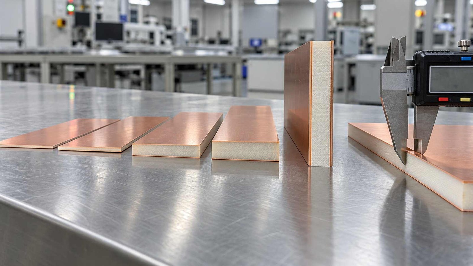
An Arlon AD255C PCB is a circuit board built on AD255C, the antenna-grade glass-reinforced PTFE laminate in the AD Series antenna materials line. The Arlon brand is now manufactured and sold by Rogers Corporation, and the current data sheet publishes the grade as AD255C: a process dielectric constant of 2.55 ± 0.05 at 10 GHz, a design Dk of 2.60, and a dissipation factor of 0.0013 at 10 GHz.
That combination — low Dk, very low loss, and a dielectric constant held to a tight tolerance — is aimed at one class of product: antennas produced in volume, where board after board has to resonate at the same frequency. The published application set is cellular infrastructure base station antennas, automotive telematics antenna systems and commercial satellite radio antennas.
This page collects the published data-sheet values for AD255C, sorts out which Dk belongs in an impedance calculation, lists the standard thickness and copper options, and covers the PIM and thermal figures that decide how the board is fabricated. The wider Arlon line — including the CLTE series — is reviewed in our Arlon high frequency PCB materials overview, and the grade-by-grade parameter view across manufacturers sits in the Rogers materials section.
1. What Is Arlon AD255C PCB?
AD255C belongs to the AD Series, a line engineered specifically for antenna markets rather than adapted to them from general-purpose microwave stock. The construction is woven glass reinforcement in a PTFE base, which is what gives the laminate its circuit processability: the glass fabric carries the mechanical load, so the board survives etch, lamination and assembly handling the way an epoxy/glass board does, while the PTFE phase provides the low loss.
Two consequences follow from that construction. First, the dielectric constant is controlled rather than merely specified — the data sheet quotes a tolerance of ± 0.05 on the process value, and tight Dk control is the property that lets element dimensions survive from lot to lot in volume antenna production. Second, the material drills, routs and plates on equipment that a high-frequency PCB factory already runs; it does not demand a separate process island.
On the naming: the grade is widely searched as Arlon AD255, and drawings still carry that callout. The current-generation designation is AD255C — older Arlon literature distinguished AD255A and AD255C variants by loss tangent and tolerance — and the parameter table to work from today is the Rogers AD Series data sheet.
2. AD255C Laminate Properties: The Datasheet Values
Everything in the table below is a published typical value from the Rogers AD Series data sheet at the test condition shown. Values that the data sheet does not state are not listed here, and nothing on this page is estimated.
| Category | Property | Typical value | Test condition |
|---|---|---|---|
| Electrical | Dielectric constant (process) | 2.55 (controlled ± 0.05) | 10 GHz, 23 °C, 50 % RH |
| Electrical | Dielectric constant (design) | 2.60 | 10 GHz, microstrip differential phase length |
| Electrical | Dissipation factor | 0.0013 | 10 GHz, 23 °C, 50 % RH |
| Electrical | Thermal coefficient of Dk | −110 ppm/°C | 0 to 100 °C, 10 GHz |
| Electrical | Volume resistivity | 7.4 × 10⁸ MΩ·cm | C96/35/90 |
| Electrical | Surface resistivity | 3.6 × 10⁷ MΩ | C96/35/90 |
| Electrical | Dielectric strength | 911 V/mil | — |
| Electrical | Dielectric breakdown | > 40 kV | X/Y direction |
| Electrical | PIM (S1 / S1R foil) | −159 / −163 dBc | 1900 MHz, 43 dBm reflected, 0.030″ & 0.060″ laminate |
| Physical | Flammability | UL 94 V-0 | — |
| Physical | Moisture absorption | 0.03 % | E1/105 + D48/50 |
| Physical | Density | 2.28 g/cm³ | 23 °C |
Published typical values for AD255C from the Rogers AD Series data sheet (Publication #92-197). Specification limits for a specific lot come from the material certificate, not from this table.
Two rows deserve attention before the rest. The loss figure of 0.0013 at 10 GHz is roughly a third of a typical filled hydrocarbon laminate and places AD255C firmly in the low-loss class for feed networks and radiating elements alike. And the moisture absorption of 0.03 % is the figure behind outdoor antenna stability — water in the substrate raises both Dk and loss, so a low absorption number is what keeps a cabinet-mounted antenna on frequency after a season of rain.
3. Process Dk vs Design Dk: Which Number Goes Into the Calculation
The AD Series data sheet publishes two dielectric constants for AD255C, and they are not two readings of the same quantity. The process Dk of 2.55 is measured by the IPC TM-650 2.5.5.5 method on a clamped stripline fixture and is the figure used for material specification. The design Dk of 2.60 is derived by the microstrip differential phase length method — that is, from real etched circuits — and it is the number a field solver should be given.
The gap between them is not noise. A real trace loads the field differently from a test fixture: fringing, copper geometry and the local field distribution all pull the effective permittivity upward. Run an impedance calculation with 2.55 and the fabricated coupon will read a few percent below the target impedance, which on an antenna element means a resonance shift that then has to be explained.
The same discipline applies to the rest of the series. The data sheet lists design values of 2.50 for AD250C, 2.94 for AD300D and 3.50 for AD350A against their process values, so whatever grade a drawing calls out, the solver figure and the specification figure should be agreed before fabrication starts. How Dk and Df propagate into loss and impedance on a finished board is treated in depth in our article on high frequency PCB materials.
| AD Series grade | Process Dk | Design Dk | Df @ 10 GHz | TCDk (ppm/°C) | Thermal conductivity W/(m·K) | CTE z-axis (ppm/°C) |
|---|---|---|---|---|---|---|
| AD250C | 2.52 | 2.50 | 0.0013 | −117 | 0.33 | 196 |
| AD255C | 2.55 | 2.60 | 0.0013 | −110 | 0.35 | 196 |
| AD300D | 2.97 | 2.94 | 0.0021 | −73 | 0.37 | 98 |
| AD350A | 3.54 | 3.50 | 0.0033 | −57 | 0.44 | 63 |
All four grades on one data sheet. The table lists parameter facts only; grade selection is a design decision made on the frequency band, the element geometry and the thermal budget of the specific board.
4. Thickness, Panel and Copper Options
On an antenna laminate, thickness is an electrical parameter long before it is a mechanical one: element size scales with Dk and dielectric thickness together, so the available gauges define what a layout can be built on. The standard offerings are listed below.
| Item | Standard offering |
|---|---|
| Dielectric thickness | 0.020″ (0.508 mm) ± 0.002″ · 0.030″ (0.762 mm) ± 0.002″ · 0.040″ (1.016 mm) ± 0.002″ · 0.060″ (1.524 mm) ± 0.002″ · 0.125″ (3.175 mm) ± 0.006″ |
| Panel size | 12″ × 18″ (305 × 457 mm) · 24″ × 18″ (610 × 457 mm) |
| Copper foil — standard | Electrodeposited (ED) copper: ½ oz (18 µm) or 1 oz (35 µm) |
| Copper foil — low PIM | Reverse-treated ED copper: ½ oz (18 µm) or 1 oz (35 µm) |
| Other configurations | Additional thicknesses, panel sizes and claddings on request from the manufacturer |
Standard offerings table of the AD Series data sheet. Availability of a specific gauge is the first thing to confirm on any new antenna build, because a thickness that is not stocked forces the element dimensions to be re-derived rather than the board simply re-quoted.
Note where the tolerance steps change. The four gauges up to 0.060 inch carry a ± 0.002 inch window, while the 0.125 inch gauge opens to ± 0.006 inch — in percentage terms a wider window, and on a design where thickness feeds directly into resonance it is worth checking whether the electrical budget absorbs it. For a feed network on a thicker build, the impedance effect can be folded into the design; for a radiating element, it usually cannot.
5. Antenna Applications: What Each One Demands From the Board
The data sheet names three application families for the AD Series. The useful part for a board designer is not the list itself but what each application imposes on the fabrication:
| Published application | What the board has to hold | Data-sheet figures that answer it |
|---|---|---|
| Cellular infrastructure base station antenna | Element-to-element repeatability across a large panel, and a feed network whose loss stays low over metres of trace | Dk tolerance ± 0.05 · Df 0.0013 @ 10 GHz · dimensional stability 0.03/0.07 mils/inch |
| Automotive telematics antenna systems | Stable resonance over the full automotive temperature range and across lot changes | TCDk −110 ppm/°C · process Dk 2.55 ± 0.05 · UL 94 V-0 |
| Commercial satellite radio antenna | A radiating surface whose frequency does not drift with absorbed moisture | Moisture absorption 0.03 % · PIM −159/−163 dBc |
The application set is quoted from the AD Series data sheet. The middle and right columns map each application to the board requirement it imposes and to the published figures that answer it.
Antenna substrate selection across manufacturers — including how AD255C sits against other low-Dk antenna laminates on parameters alone — is compared in our guide to PCB materials for antenna applications. Array-level design, where Dk uniformity across a panel matters more than the absolute value, is covered in the phased array PCB review, and fabrication of the radiating structure itself is described on our antenna PCB product page.
6. PIM: Why the Copper Foil Choice Decides It
Passive intermodulation is the failure mode that antenna production cares about and most board design guides ignore. A base station antenna transmits at high power while the receive chain listens two frequencies away; any nonlinearity in the RF path — a contaminated interface, a ferromagnetic inclusion, a rough foil with current crowding — mixes the two carriers into interference that lands exactly in the receive band.
The AD Series data sheet publishes PIM as a tested figure, not a marketing claim: −159/−163 dBc, measured with 43 dBm reflected swept tones at 1900 MHz on 0.030 inch and 0.060 inch laminate, using S1 and S1R foil respectively. The data sheet also states plainly that PIM performance is heavily influenced by the copper choice. That is why the standard offerings list both standard ED foil and reverse-treated ED foil at the same two weights: the reverse-treated foil presents a low-profile copper surface to the dielectric, which reduces conductor loss and, with it, the PIM contribution of the trace itself.
For the fabrication side, the practical implications are specific. Surface preparation on the radiating side, mask-free zones and clean handling all matter more on a PIM-limited build than on a generic RF board, because contamination and mechanical stress in the finished assembly are the residual PIM sources once the laminate and foil are right. The ground structure around radiating elements matters too; the stitching rules are set out in our via fence PCB guide.

7. Thermal and Mechanical Behaviour Through Fabrication
PTFE laminates are soft compared with epoxy/glass, and the fabrication plan has to respect that. The thermal and mechanical columns of the data sheet describe how the material behaves under exactly the conditions a build imposes: reflow temperatures, lamination pressure, and the dimensional drift between imaging and etch.
| Property | Typical value | Test condition |
|---|---|---|
| Decomposition temperature (Td) | > 500 °C | 5 % weight loss, 2 h @ 105 °C |
| CTE — x axis | 34 ppm/°C | −55 °C to 288 °C |
| CTE — y axis | 26 ppm/°C | −55 °C to 288 °C |
| CTE — z axis | 196 ppm/°C | −55 °C to 288 °C |
| Thermal conductivity | 0.35 W/(m·K) | z direction, ASTM D5470 |
| Time to delamination | > 60 minutes | as-received, 288 °C |
| Copper peel strength | 2.4 N/mm (13.6 lbs/in) | 10 s @ 288 °C, 35 µm foil |
| Flexural strength (MD/CMD) | 60.7 / 44.1 MPa | 25 °C, ASTM D790 |
| Tensile strength (MD/CMD) | 55.8 / 45.5 MPa | 23 °C, 50 % RH |
| Flexural modulus (MD/CMD) | 6,412 / 5,640 MPa | 25 °C |
| Dimensional stability (MD/CMD) | 0.03 / 0.07 mils/inch | after etch + bake |
| Specific heat capacity | 0.813 J/(g·K) | 2 h @ 105 °C |
Thermal and mechanical columns of the same data sheet. On an antenna panel the two rows that matter most in fabrication are the Z-axis CTE, which sets plated-barrel strain through reflow cycles, and dimensional stability, which sets how much the etched artwork moves between imaging and lamination.
Two rows drive the fabrication decisions. The Z-axis CTE of 196 ppm/°C is the figure that sets how much a plated barrel is strained on each trip through reflow — relevant on any multilayer that combines AD255C layers with thermally different cores, which is the normal case in a FR4 Rogers hybrid PCB build where the antenna layers carry the RF and FR-4 carries the digital and power wiring. And the dimensional stability figure of 0.03/0.07 mils per inch after etch and bake is what the artwork compensation has to be planned around on a large panel, because a 610 mm panel that moves even a little shifts every element on it.
Drill and rout parameters for glass/PTFE laminates are a shop capability question as much as a material one; our high frequency PCB drilling capabilities note covers what the line has to be set up to do.
8. Manufacturing AD255C Boards: What to Send and What We Check
Most of the risk on an AD255C build is settled before the first panel is imaged, in the exchange between the designer and the factory. The checklist below is what we work through when quoting.
| What we confirm before fabrication | Why it matters on AD255C |
|---|---|
| Gauge and copper weight against the element dimensions | Element size scales directly with Dk and thickness; a substitution changes the resonance, not just the price |
| Foil type: ED vs reverse-treated ED | PIM is foil-dominated on this material; the data-sheet PIM figures are quoted for S1 and S1R foil specifically |
| Mask and surface finish on the radiating side | Solder mask over radiating elements shifts resonance; mask-free radiating areas need the finish chosen for loss, not just for cost |
| Impedance targets with the design Dk agreed in writing | Design Dk 2.60 is the solver value; agreeing the figure prevents a coupon-versus-simulation argument later |
| Lamination and drill parameters for PTFE/glass | PTFE laminates need their own drill and desmear settings; the line has to be set up for the material, not for epoxy/glass |
| Flatness on large thin panels | A 0.020″ core on a 610 × 457 mm panel needs handling and fixturing planned before the build, not during it |
The list we work through when quoting an antenna build on AD255C. None of it is material-specific wizardry; it is the difference between quoting a laminate and manufacturing a working antenna board.
Send the Gerbers with the stackup, the impedance targets and the PIM requirement if the build has one, and we will confirm the gauge, foil type and fabrication route before anything is cut. If the design is still at the material-selection stage, the full laminate landscape is indexed in our high frequency PCB materials section.
Arlon AD255C PCB — Frequently Asked Questions
The AD255 naming, which Dk goes into the calculation, standard thicknesses, and why the grade sits on base station antennas.
Is Arlon AD255 the same material as AD255C?
AD255 is the base grade designation from the original Arlon AD Series literature, which also listed AD255A and AD255C variants with lower loss tangent and tighter tolerance. Arlon is now part of Rogers Corporation, and the current Rogers AD Series data sheet lists the grade as AD255C, with AD250C, AD300D and AD350A alongside it. In practice, drawings that call out Arlon AD255 are quoted against AD255C, and the parameter table to check is the current data sheet rather than the older Arlon one.
Which Dk should I use for an impedance calculation on AD255C?
The design Dk of 2.60. The data sheet publishes a process Dk of 2.55 at 10 GHz as the material specification figure, and a design Dk of 2.60 derived by the microstrip differential phase length method. The two numbers describe different things: the process value is for lot-to-lot material comparison, while the design value is what a real etched trace presents to the field. A field solver run with the process value understates the geometry loading, and measured impedance then comes in below target on the coupon.
What thicknesses and copper weights does AD255C come in?
Standard dielectric thicknesses are 0.020, 0.030, 0.040, 0.060 and 0.125 inch (0.508, 0.762, 1.016, 1.524 and 3.175 mm), on 12 × 18 inch and 24 × 18 inch panels. Copper cladding is electrodeposited foil at ½ oz (18 µm) or 1 oz (35 µm), with the same two weights offered in reverse-treated ED foil for lower-loss, lower-PIM builds. Other configurations exist but are request items, so a gauge outside the standard list should be confirmed before a layout is frozen.
Why is AD255C specified for base station antennas?
Because antenna production fails commercially on repeatability before it fails electrically. The grade publishes a dielectric constant tolerance of ± 0.05, a dissipation factor of 0.0013 at 10 GHz for low feed-network loss, a PIM figure of −159/−163 dBc measured with S1 and S1R foil, and a moisture absorption of 0.03 % so the resonance does not drift outdoors. Combined with a thermally stable PTFE/glass system (Td above 500 °C), those figures address the exact mechanisms that cause antenna yield loss in volume production.
Building an antenna board on AD255C?
Send us the band, the dielectric thickness and the foil type you have in mind. We will confirm the gauge against the current standard offerings, agree the Dk figure to be used for the impedance target, and quote fabrication with coupon TDR data on the lot we actually build from.
Contact Us → WhatsApp: +86 137 6047 3650Request a PCB Quote
Upload your Gerber ZIP file and project requirements. Our engineering team will review your PCB material, stackup, impedance needs, surface finish, and production quantity before quoting.
Please prepare:
- Gerber files in ZIP format
- PCB material or stackup requirements
- Controlled impedance notes if available
- Prototype or batch production quantity