
Board-to-Board RF Connector PCB: Solderless 40 GHz Transitions, Coplanarity and Phase
Board-to-board RF connector PCB guide: solderless 40 GHz transitions, coplanarity tolerance chains, tolerance-to-phase arithmetic and gold skin-depth limits.
Home » 40 GHz PCB » Board-to-Board RF Connector PCB: Solderless 40 GHz Transitions, Coplanarity and Phase
Table of Contents
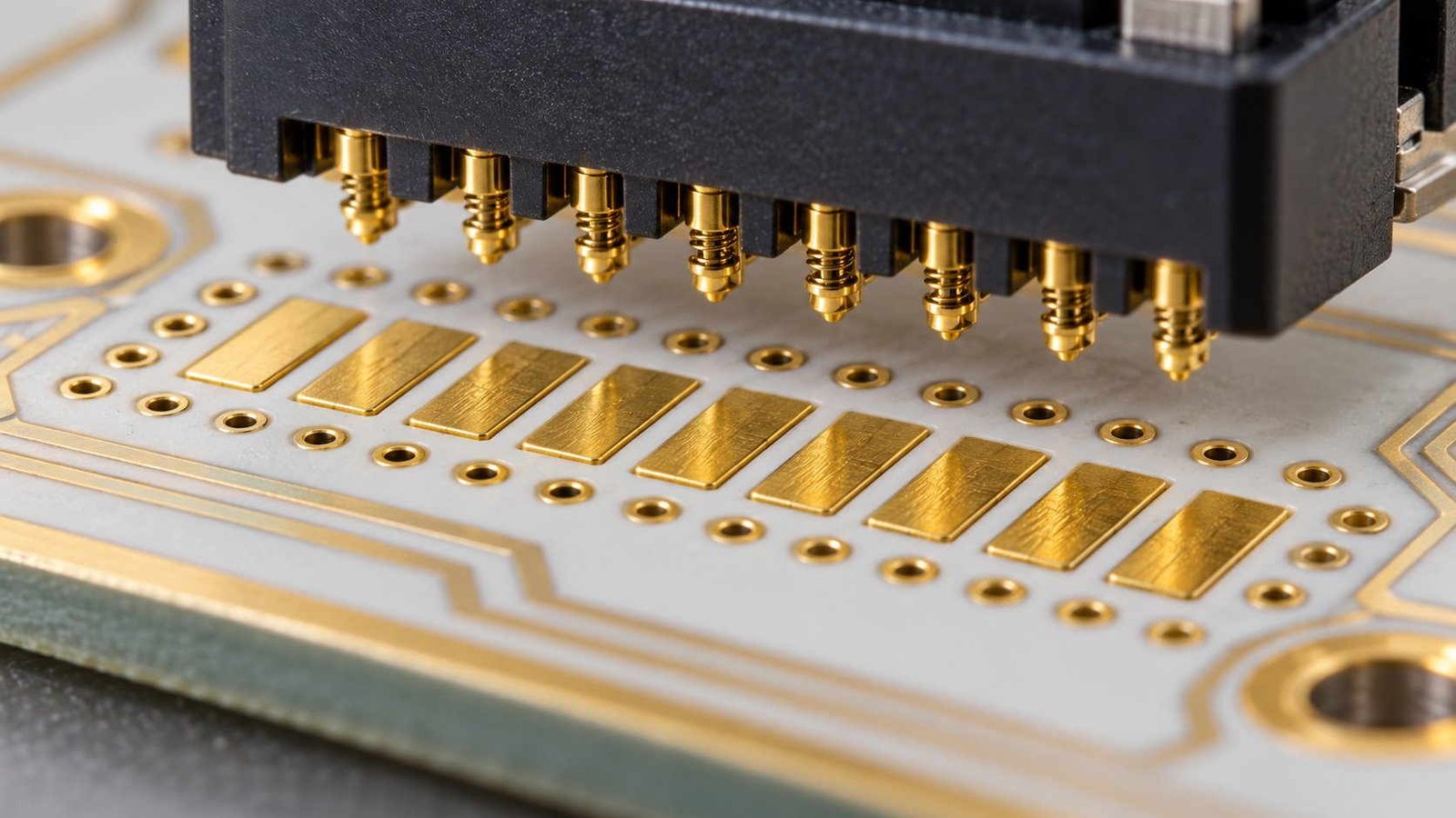
At EuMW 2026 the board-to-board interconnect stopped being a cable assembly and became a component: spring-contact families rated to 40 GHz in two, four, six and eight channels, on a 3 mm pitch, with a 3.3 mm board-to-board height, mated by pressing one board onto the other — no solder, no mating connector pair, no cable. That is a clean mechanical idea. It is also, quietly, a transfer of responsibility: with no solder joint and no cable, the last controlled impedance in the system is the pad on your board.
This page works through the numbers that decide whether such a board works: how electrically long 3.3 mm of spring contact really is; how seven independent tolerances compare with the travel of a spring; how a length tolerance in microns becomes a beam-steering error in degrees; why a gold layer that is adequate at 40 GHz can be inadequate at 1 GHz; what 3 mm of pitch buys in isolation and what it costs; and how many ground vias it takes before a shield is a shield.
The horizontal case — a coaxial connector launching into a trace — is covered in our RF connector launch PCB guide, and the impedance method itself in the controlled impedance PCB guide. This page is about the vertical case, where geometry rather than impedance is the binding constraint.
1. A Spring Contact Is a Length of Coax, Not a Pin
Drawings show a spring contact as a pin with a force specification. Electrically it is a short coaxial line with two step discontinuities.
| Frequency | λ0 in air | 3.3 mm as electrical length | What the transition is |
|---|---|---|---|
| 10 GHz | 29.98 mm | 11.0% λ | A short segment; lumped contact models still work |
| 20 GHz | 14.99 mm | 22.0% λ | A visible line — impedance steps start to show |
| 28 GHz | 10.71 mm | 30.8% λ | Must be designed as a transmission line |
| 40 GHz | 7.49 mm | 44.0% λ | Nearly half a wavelength — the barrel is the device |
| 67 GHz | 4.47 mm | 73.8% λ | Beyond this page’s design range; resonance, not contact, sets the limit |
A spring contact is normally drawn as a pin and specified as a force. Electrically it is a short length of coaxial line: pad, barrel, pin, and a ground ring around all three. At 3.3 mm stack height that line is 44% of a wavelength at 40 GHz, so what sets the transition is the local impedance of the barrel and the two step discontinuities at its ends — not the contact resistance. The pad annulus, the ground ring and the via pattern behind it are the line.
At the 3.3 mm stack height these connectors use, the transition is 44% of a wavelength at 40 GHz. Nothing about that is lumped: the pad annulus, the barrel and the ground ring form a line whose impedance is set by the ring diameter and the dielectric around it, and the pad-to-barrel step is a discontinuity that radiates and reflects in proportion to how abrupt it is. Which means the footprint is not a landing zone for a contact — it is the last impedance-controlled structure on the board, and it deserves the same stackup review as the trace feeding it.
2. Coplanarity Is the Real 40 GHz Specification
Every spring needs to be compressed, and every spring has a range. On a blind-mate stack, whether that range is respected is decided by the board, not by the connector.
| Tolerance item | Uncontrolled board ± mm | Controlled board ± mm | Share of the uncontrolled worst case |
|---|---|---|---|
| Laminate thickness (1.6 mm) | 0.160 | 0.050 | 34.8% |
| Board-to-board standoff height | 0.100 | 0.030 | 21.7% |
| Pad-to-locating-hole registration | 0.075 | 0.040 | 16.3% |
| Connector seating plane | 0.050 | 0.020 | 10.9% |
| Flatness over a 30 mm footprint | 0.050 | 0.015 | 10.9% |
| Finished pad height (copper + gold) | 0.015 | 0.015 | 3.3% |
| Solder-mask dam at the pad edge | 0.010 | 0.010 | 2.2% |
The uncontrolled column is what a standard 1.6 mm laminate stack delivers when nobody asks for anything: ±10% on thickness alone, ±0.10 mm on standoffs. The controlled column is what a pressed stack with a machined standoff and laser-drilled locating holes delivers. Two of the smallest items are the ones factories forget: the finished pad height and the solder-mask dam, because both sit directly under the spring tip.
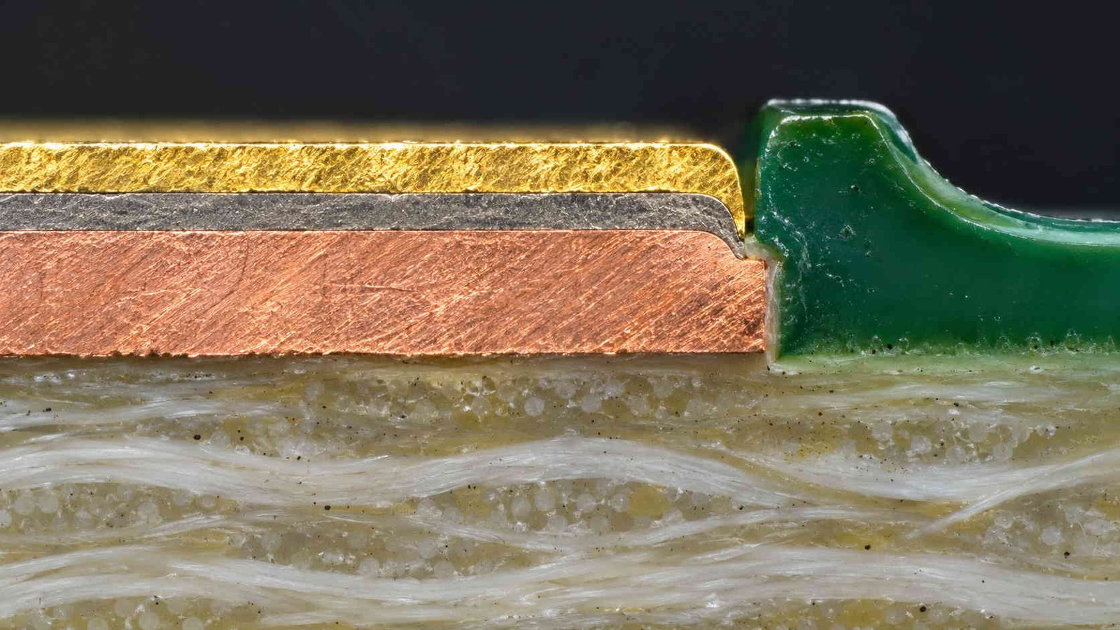
Read the last three rows closely, because they are the ones nobody puts on a drawing. The finished pad height is copper plus gold: 18 µm of copper on an inner layer is already 9% of the stroke. The solder-mask dam is 25 µm, and if it is allowed to sit at the pad edge it lifts one contact out of a coplanar plane that was measured perfectly at the CMM. Between the two of them, a board can pass every inspection and still fail on the eighth channel.
3. Does the Spring Travel Actually Cover It?
Sum the chain and compare it with the stroke. This is the single calculation that separates a board-to-board design that works from one that is quoted and then debugged.
| Configuration | Worst-case sum | Statistical sum (RSS) | Against ±0.20 mm of usable spring travel |
|---|---|---|---|
| Uncontrolled board, worst case | 0.460 mm | — | 230% — 0.26 mm past the stop, contacts lift or bottom out |
| Uncontrolled board, RSS | — | 0.216 mm | 108% — fails even statistically |
| Controlled board, worst case | 0.180 mm | — | 90% — fits, with 0.02 mm to spare |
| Controlled board, RSS | — | 0.077 mm | 39% — 61% of the travel left for assembly |
This is the table that decides whether a board-to-board design works, and it explains why the specification has to be written statistically. A worst-case sum of seven independent tolerances almost never fits a spring stroke; an RSS sum is what actually happens on a production line, provided the processes are centred and the distributions are not skewed. The uncontrolled board fails both ways. Board thickness alone consumes 80% of a ±0.20 mm stroke before anything else is counted, and a 25 µm solder-mask dam is 6% of the stroke on its own — small, but it is the item that shows up as one intermittent channel rather than a failed lot.
The uncomfortable conclusion is that a worst-case summation almost never closes, and a design that demands it will be over-specified on every other axis. What closes is the statistical sum — the RSS — and it only closes if the processes are centred. Which is why the answer to "how flat?" is never a single tolerance: it is a stackup and a process capability, and it is decided at quotation, before the first panel is laminated. Laminates and their thickness options are set out in our high-frequency PCB materials review and the selection arithmetic in the PCB material comparison chart.
4. Microns Become Degrees
In a single-channel link, a tenth of a millimetre of length difference is nothing. In an eight-channel bank it is beam-steering error.
| Channel-to-channel length spread | Phase at 28 GHz | Phase at 40 GHz | In 5-bit phase-shifter LSBs (11.25°) at 40 GHz |
|---|---|---|---|
| ±0.05 mm (0.10 mm p-p) | 10.0° p-p | 7.1° p-p | 0.6 LSB — inside one step |
| ±0.10 mm (0.20 mm p-p) | 19.9° p-p | 14.2° p-p | 1.3 LSB — one step of steering error |
| ±0.20 mm (0.40 mm p-p) | 39.9° p-p | 28.5° p-p | 2.5 LSB — the beam points somewhere else |
| ±0.50 mm (1.00 mm p-p) | 99.7° p-p | 71.2° p-p | 6.3 LSB — aperture is no longer coherent |
In PTFE-class laminate one millimetre of line is 49.9° at 28 GHz and 71.2° at 40 GHz, so the length spread across a channel bank converts directly into beam-steering error. This is the quiet reason an eight-channel connector is harder than eight single-channel launches: the same mechanical tolerance that was invisible at 6 GHz is more than one phase-shifter step at 40 GHz. Wavelength values use εr = 2.2 as a stated assumption; the ratio, not the absolute number, is the argument.
The arithmetic is unforgiving because wavelength is short and phase is linear in length. At 40 GHz, one millimetre of PTFE-class line is 71°: a routing spine that differs by 0.1 mm between channel one and channel eight shifts that channel by more than one step of a 5-bit phase shifter. Nobody notices this at 6 GHz, where the same 0.1 mm is 7°. The factory consequence is that length matching has to be measured and reported per channel — the same discipline as impedance, applied to a different quantity.
5. Gold, Nickel and the Skin-Depth Trap
Finish specifications are usually written for the highest frequency on the board. For a spring-contact footprint, that is the wrong instinct.
| Frequency | δ in gold | 0.05 µm gold (ENIG minimum) | 0.10 µm gold (ENIG typical) | 0.50 µm gold (soft gold) | 1.50 µm gold (hard gold) |
|---|---|---|---|---|---|
| 1 GHz | 2.49 µm | 0.02δ — nickel carries the current | 0.04δ — nickel carries the current | 0.20δ — still nickel-dominated | 0.60δ — now gold-dominated |
| 10 GHz | 0.79 µm | 0.06δ | 0.13δ | 0.64δ | 1.91δ |
| 40 GHz | 0.39 µm | 0.13δ | 0.25δ | 1.27δ — adequate | 3.82δ |
| 67 GHz | 0.30 µm | 0.16δ | 0.33δ | 1.65δ | 4.94δ |
Skin depth falls as frequency rises, which produces a result that surprises most drawings: a 0.5 µm gold layer is 0.20δ at 1 GHz but 1.27δ at 40 GHz. Thin gold is electrically adequate at millimetre-wave frequencies and inadequate at low GHz, where the field reaches the nickel underlayer. A board that carries an L-band calibration or control path alongside its 40 GHz channels therefore has to be finished for the lowest frequency in the stack, not the highest. Nickel’s permeability makes the low-frequency case worse than its resistivity alone suggests, and the same nickel layer is what wears during mating — which is why wiping contacts are normally hard gold over 3–5 µm nickel rather than thin ENIG.
The table says something that reads backwards until you see the mechanism: skin depth shrinks as frequency rises, so a thin gold layer is fine at 40 GHz and transparent at 1 GHz. Current crowds into the surface at high frequency and stays in the gold; at low frequency it spreads down into the nickel, which is roughly four times more resistive and, being magnetic, worse than that number implies. A board carrying L-band calibration lines and a 40 GHz channel in the same stack therefore cannot be finished for the 40 GHz channel alone. Wiping contacts add wear to the requirement, which is why these footprints tend to end up as hard gold over nickel rather than thin ENIG. The finish families are compared in our surface finish for RF and microwave PCB guide and the ENIG-versus-ENEPIG arithmetic in the ENIG vs ENEPIG vs immersion silver comparison.
6. Three Millimetres of Pitch: What the Shield Buys
Why build each channel as its own coaxial barrel instead of running eight pins in a row? The pitch answers it.
| Centre-to-centre pitch | Coupling capacitance | Reactance at 40 GHz | Unshielded near-end coupling |
|---|---|---|---|
| 0.75 mm | 11.69 fF | 340 Ω | 22.7 dB — unusable without a shield |
| 1.50 mm | 5.84 fF | 681 Ω | 28.7 dB — fails a 30 dB isolation target |
| 3.00 mm | 2.92 fF | 1362 Ω | 34.7 dB — the connector’s own pitch |
| 6.00 mm | 1.46 fF | 2724 Ω | 40.7 dB — meets a 40 dB target unshielded |
| 12.00 mm | 0.73 fF | 5447 Ω | 46.8 dB |
This is an order-of-magnitude model, not a field solve: the coupling area is taken as a 0.3 mm contact over the 3.3 mm parallel run, and the estimator is a lumped capacitive divider into 50 Ω. It says two things. First, at the 3 mm pitch these connectors use, an unshielded pin pair lands around 35 dB — which is precisely why each channel is built as its own coaxial barrel. Second, the shield only buys that isolation if its ground ring is genuinely grounded at the pad, which is the subject of the next table.
An unshielded pair at 3 mm lands around 35 dB at 40 GHz — usable, but with nothing left for a 40 dB isolation target, and with no margin for the eight-channel case where every aggressor has seven neighbours. The barrel is what buys the rest. But a shield is a conductor with two ends, and its effectiveness at 40 GHz is set by how well the ground ring at the pad behaves.
| Ground-ring vias per channel | Inductance | Reactance at 40 GHz | Versus the 50 Ω signal path |
|---|---|---|---|
| 1 via | 0.539 nH | 135 Ω | 2.7× the signal impedance — a stub, not a shield |
| 2 vias | 0.269 nH | 68 Ω | 1.4× — marginal |
| 4 vias | 0.135 nH | 34 Ω | 0.7× — shield starts to work |
| 6 vias | 0.090 nH | 23 Ω | 0.5× — the useful minimum |
| 8 vias | 0.067 nH | 17 Ω | 0.3× — diminishing returns |
Inductance is computed for 0.3 mm drilled vias, 0.8 mm from the pad to the first ground plane. A single-via ground ring is the most common defect in high-frequency connector footprints: it looks connected on a netlist, and at 40 GHz it leaves the barrel floating on 135 Ω of reactance, which returns the channel to the unshielded crosstalk number in the previous table. The ring also has to be free of solder mask — a mask-covered ground ring is an insulator with a nice drawing.
Six vias, not one. A single 0.3 mm via is 0.54 nH — 135 Ω at 40 GHz, which is 2.7 times the signal impedance; the barrel is then referenced to a floating ring and the crosstalk returns to the unshielded baseline. This is the most common defect in a high-frequency connector footprint because it passes every netlist and continuity check. It is also the kind of detail that only matters in banks: eight channels in a row concentrate the mistake. Multi-channel applications that live or die on this discipline are treated in our phased array PCB guide.
7. What Can Only Be Measured Before the Stack Is Closed
A blind-mate stack is inspected before it exists and after it is sealed, and never in between.
| Record to request | What it proves | Why it cannot be recovered afterwards |
|---|---|---|
| Pad-plane CMM or laser scan over the connector footprint, with the locating holes as datum | Coplanarity to the seating plane, per pad | Once the connector is pressed on, the pads are hidden and the gap is set |
| Solder-mask dam height and mask-free ring check | No mask lifting a spring tip | A 25 µm dam is invisible under a pressed contact |
| Cross-section of the pad finish: gold and nickel thickness | The finish the loss calculation assumed | Destructive; cannot be sampled from a delivered assembly |
| Pad-to-hole registration report, with Cpk over the lot | Blind-mate alignment before the spring takes over | Misalignment shows as a mating force problem at the customer, not at the factory |
| Warpage after two reflow cycles, measured with the assembly fixture | The flatness the standoffs will see | As-delivered warpage is measured before the assembly has been through reflow |
| Per-channel electrical length report | The phase spread the beam former has to live with | Cannot be measured once the boards are stacked |
| S-parameters of a launch coupon with the actual connector family | The transition, not just the trace | The coupon exists only in the fabrication lot |
| Mating force and compression record on first article | That the springs are inside their working range | Force is a first-mate property; later mates tell a different story |
Board-to-board hardware is assembled and then closed: after that, neither the pad plane nor the ground ring can be inspected, and every parameter that decides performance is set by geometry produced in fabrication. The records above are what a fabrication lot can hand over before that door closes.
The pattern is the same as in any buried-structure problem: the parameters that decide the outcome are produced in fabrication and consumed in assembly, so the only defence is a first-article package that records them while they are still visible. Measurement method matters as much as the record — the launch coupon is only meaningful if it carries the real connector family, which is the same argument we make about calibration coupons in the 110–145 GHz calibration board work, and the de-embedding reference plane is set out in the RF and mmWave test fixture PCB design guide and the mmWave PCB VNA testing guide.
8. The Board-to-Board RFQ Checklist
Eight lines, each traceable to a number computed above or a mechanism that cannot be recovered after assembly.
| # | Drawing or PO line item | Why it is on the list |
|---|---|---|
| 1 | Pad plane tolerance stated against a seating plane, with the datum called out | The tolerance chain only closes if everyone measures from the same plane (section 2) |
| 2 | Laminate thickness tolerance and the pressed-stack construction | ±10% thickness alone consumes 80% of the spring travel (section 2) |
| 3 | Standoff height and its tolerance, plus the flatness the assembly is bolted to | The board-to-board gap is part of the RF path, not just mechanics (section 2) |
| 4 | Ground-ring via count and pattern per channel, mask-free ring width | One via leaves 135 Ω of ground reactance at 40 GHz (section 5) |
| 5 | Finish specified by gold thickness and hardness, not by finish name | 0.5 µm gold is adequate at 40 GHz and inadequate at 1 GHz (section 4) |
| 6 | Per-channel length matching target, with the measurement method | 0.1 mm is 14° at 40 GHz — one phase-shifter step (section 3) |
| 7 | Warpage limit after reflow simulation, with the fixture defined | As-delivered flatness is not the flatness the assembly sees (section 6) |
| 8 | First-article package: CMM, cross-section, registration Cpk, launch coupon data, mating force | None of it can be recovered after the boards are stacked (section 6) |
Eight lines. Items 1–3 decide whether every spring lands inside its travel; 4–5 decide whether the transition and the shield behave as modelled; 6–8 decide whether anyone can prove either after the assembly is closed. A board-to-board RFQ carrying these answers is quoted on engineering, not on price.
The pattern: a solderless board-to-board interface is specified by geometry and proved by records. The connector vendor owns the spring; the board owns everything the spring touches.
Board-to-Board RF Connector PCB — Frequently Asked Questions
How a vertical spring contact differs from a coaxial launch, the coplanarity stack-up, thickness tolerance, gold thickness at 40 GHz, and ground-ring vias.
What is different about a board-to-board RF connector PCB compared with a coaxial launch?
Direction. A coaxial launch brings a cable in horizontally and the design problem is the transition from connector to trace: pad geometry, ground cut-out, stub length. A board-to-board interconnect goes vertically through a stack, so the same board carries two sets of pads facing each other with 3.3 mm of spring contact between them. That changes the binding constraint from impedance to geometry: pad-plane coplanarity, standoff tolerance, registration and per-channel length all become part of the RF path, and none of them can be inspected after the assembly is closed.
How flat do the contact pads actually have to be?
Flat enough that every spring sits inside its working range, which is a stack-up question rather than a single number. Seven tolerances decide it: laminate thickness, finished pad height, solder-mask dam, connector seating plane, pad-to-hole registration, flatness over the footprint, and standoff height. On a standard stack the worst-case sum is 0.46 mm against a ±0.20 mm spring travel — 230% of the stroke. Tighten thickness to ±0.05 mm, flatness to ±0.015 mm and standoffs to ±0.03 mm and the statistical sum falls to 0.077 mm, leaving 61% of the travel as margin.
Why does laminate thickness tolerance matter so much?
Because it is the largest single term and it moves the pad plane directly. A 1.6 mm laminate at ±10% is ±0.16 mm, which is 80% of a ±0.20 mm spring stroke before any other tolerance is counted. Specifying a pressed stack at ±0.05 mm is usually the cheapest single change available, and it is a fabrication decision rather than a design change.
Is 0.5 µm of gold enough for a 40 GHz channel?
At 40 GHz, yes — skin depth in gold is about 0.39 µm, so a 0.5 µm layer carries 1.27 skin depths and the current stays essentially in gold. At 1 GHz the same layer is only 0.20 skin depths, and the field reaches the nickel underneath, which is both more resistive and magnetic. So the answer depends on the lowest frequency on the board, not the highest. Wiping contacts add a second requirement: wear resistance, which is why hard gold over 3–5 µm nickel is the usual choice for a connector that will be mated repeatedly.
What should the drawing say about ground vias at the connector footprint?
A count and a pattern, not just continuity. Six 0.3 mm vias on a ground ring give about 0.09 nH, or 23 Ω at 40 GHz; a single via gives 135 Ω, which is 2.7 times the signal impedance and turns the shield into a stub. The ring should also be mask-free around the full circumference — a mask-covered ground ring is electrically an insulator, and it looks perfectly connected on a netlist.
Designing a blind-mate board stack for 40 GHz?
Send the connector footprint, the pad-plane requirement, the standoff arrangement and your length-matching target. We will close the tolerance chain against the spring travel, set the ground-ring via pattern, specify the finish by thickness and hardness, and ship the first-article package — CMM pad plane, cross-section, registration Cpk, per-channel length and launch coupon data — with the boards to IPC Class 3.
Contact Us → WhatsApp: +86 137 6047 3650Request a PCB Quote
Upload your Gerber ZIP file and project requirements. Our engineering team will review your PCB material, stackup, impedance needs, surface finish, and production quantity before quoting.
Please prepare:
- Gerber files in ZIP format
- PCB material or stackup requirements
- Controlled impedance notes if available
- Prototype or batch production quantity