
Embedded Resistor PCB: Thin-Film Resistive Foil for Millimetre-Wave Boards
Embedded resistor PCB guide: thin-film resistive foil for millimetre-wave boards, parasite arithmetic, pad values, etch tolerance and fabrication acceptance.
Home » Buried Resistor PCB » Embedded Resistor PCB: Thin-Film Resistive Foil for Millimetre-Wave Boards
Table of Contents
At millimetre-wave frequencies, the humble chip resistor runs out of road. Not because its resistance drifts — because its pads, solder joints and return path become significant fractions of a wavelength, and its parasitic inductance overtakes the resistance it was bought for. The industry’s answer is to stop mounting the resistor at all: put a resistive film inside the laminate and let the etching step form the resistor as part of the trace.
That capability was on display at EuMW 2026, where a resistive-foil maker presented its thin-film resistor-conductor families — including an ultra-low-profile copper variant aimed squarely at microwave and millimetre-wave loss — and reported custom attenuator and equalizer samples tested to 40 GHz. This page computes what that means at board level: what a discrete resistor actually contributes at 28 GHz, what the foil gives you, what values and tolerances are reachable, and which fabrication records the acceptance of a buried passive now rests on. Every figure is computed; assumptions are stated where they are used.
The neighbouring topics are treated separately: trace-level impedance method in our controlled impedance RF PCB and 50 ohm RF trace guides, and the measurement side in the mmWave PCB VNA testing guide. This page is about the resistor itself — the one you stop buying and start etching.
1. The Discrete Resistor at mmWave: a Parasite Story in Four Numbers
The case for embedding is arithmetic, not fashion. Take a 0402-class chip resistor and add up what comes with it.
| Frequency | Series reactance of a 0402-class chip resistor (ESL ≈ 0.4 nH) | As a fraction of a 50 Ω system |
|---|---|---|
| 3.5 GHz | 8.8 Ω | 18% — measurable, still tolerable |
| 10 GHz | 25 Ω | 50% — the pad + solder joint is already a half-impedance series element |
| 28 GHz | 70 Ω | 141% — the “resistor” is now mostly an inductor |
| 40 GHz | 100 Ω | 201% — unusable as a circuit element |
XL = 2πfL with a 0.4 nH equivalent series inductance — an industry-typical figure for a 0402-class thin-film chip resistor with its pads and solder joints (stated assumption). An embedded thin-film resistor has none of this chain: the resistive region sits inside the trace itself, with no pads, no solder joints and no extra return-path vias. At Ka band the discrete part is not a degraded solution — it is a different component.
The 28 GHz row is the decision point: at 70 Ω of series reactance, the “50 Ω resistor” is mostly inductor. Every discontinuity you remove — pads, joints, the via that returns the current to ground — is parasitic budget recovered. An embedded thin-film resistor keeps only the part that does the work: a region of resistive film, defined by geometry, living inside the trace.
2. The Material: Resistive Foil, Not a Component
The material is deceptively simple: a resistive alloy layer on copper foil, laminated foil-down like any other copper-clad laminate.
| Resistive foil property | Typical published class | What the fabricator inherits |
|---|---|---|
| Construction | NiP-type resistive alloy layer on copper foil, laminated foil-down | The resistor is formed by etching the copper — one extra etch step, not one extra process |
| Sheet resistance classes | 25 / 50 / 100 Ω/sq are the typical published classes | One laminate can carry several resistance values — geometry, not component selection, sets each value |
| mmWave foil option | Ultra-low-profile copper foil class (TCR-EHF is the reported example) | At 28–40 GHz conductor loss is roughness-limited — the foil finish is a loss spec |
| Temperature coefficient | Tens of ppm/°C class for NiP-type films (typical) | Amplitude-flat behaviour across temperature — the reason equalizers work as etched |
Ohmega Ticer presented the OhmegaPly, TCR and TCR-EHF families at EuMW 2026 and reported custom attenuator and equalizer samples tested to 40 GHz — reported figures, quoted as such. The classes above are industry-typical values for context; for any build, quote the foil by source, sheet resistance, tolerance, copper roughness and traceability. Material families and selection logic are treated in our high-frequency PCB materials review and the PCB material comparison chart.
Two consequences follow. First, the resistor is formed by the same etching logic as the rest of the board — one additional etch step, not one additional process. Second, for millimetre-wave builds the foil choice matters twice: the sheet class sets the resistance palette, and the copper roughness class sets the loss, which at 28–40 GHz is roughness-limited. Material families and selection logic are set out in our high-frequency PCB materials review and the PCB material comparison chart.
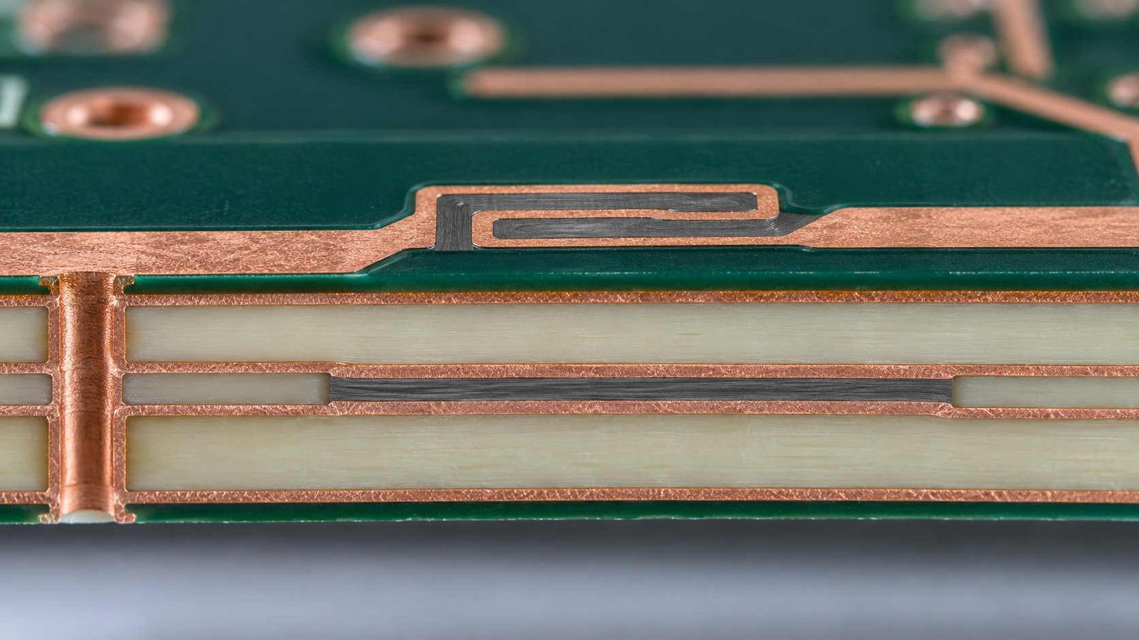
3. Geometry: the Resistor That Lives Inside the Trace
Embedding is often sold as miniaturisation, but the stronger argument is physical scale.
| Frequency (microstrip, εeff ≈ 2.6) | λ/4 | What fits inside a quarter wave |
|---|---|---|
| 10 GHz | 4.65 mm | A discrete pad + joint chain is still small against the wavelength |
| 28 GHz | 1.66 mm | Pad + solder joint + return via ≈ a quarter wavelength — the physical size of the discrete chain is now a circuit element |
| 40 GHz | 1.16 mm | Only a fully integrated resistive region behaves predictably |
λg = c/(f·√εeff) with εeff 2.6, a microstrip class on a 3.48 laminate (stated assumption). The comparison is physical, not statistical: at 28 GHz the footprint of a chip resistor assembly is the same order as a quarter-wave matching section, so its parasitics are no longer a correction term in the model — they are the model.
At 28 GHz, a chip resistor assembly — pad, part, solder joints, return via — occupies roughly a quarter wavelength of board. Its parasitics are not correction terms in the model; they are the model. The embedded equivalent is a shaped region inside a trace that already exists, with its dimensions carried on the same tolerance chain as the controlled-impedance routing around it. Satellite and phased-array front ends — the classic customers of this technique — are treated in our satellite communication PCB review and the phased array PCB guide.
4. Exact Values, Etched Not Stocked
The quietest advantage of embedded resistors is not size — it is the value set.
| π-pad 3 dB arm (Z0 = 50 Ω) | Exact value | In sheet-resistance squares |
|---|---|---|
| Series arm | 17.61 Ω | 0.70 sq @ 25 Ω/sq · 0.35 sq @ 50 Ω/sq · 0.18 sq @ 100 Ω/sq |
| Shunt arm | 292.4 Ω | 11.70 sq @ 25 Ω/sq · 5.85 sq @ 50 Ω/sq · 2.92 sq @ 100 Ω/sq |
| Nearest E24 chip to 17.61 Ω | 18 Ω = +2.2% value error | Stacked chips to reach the value would add back the parasitics this scheme exists to remove |
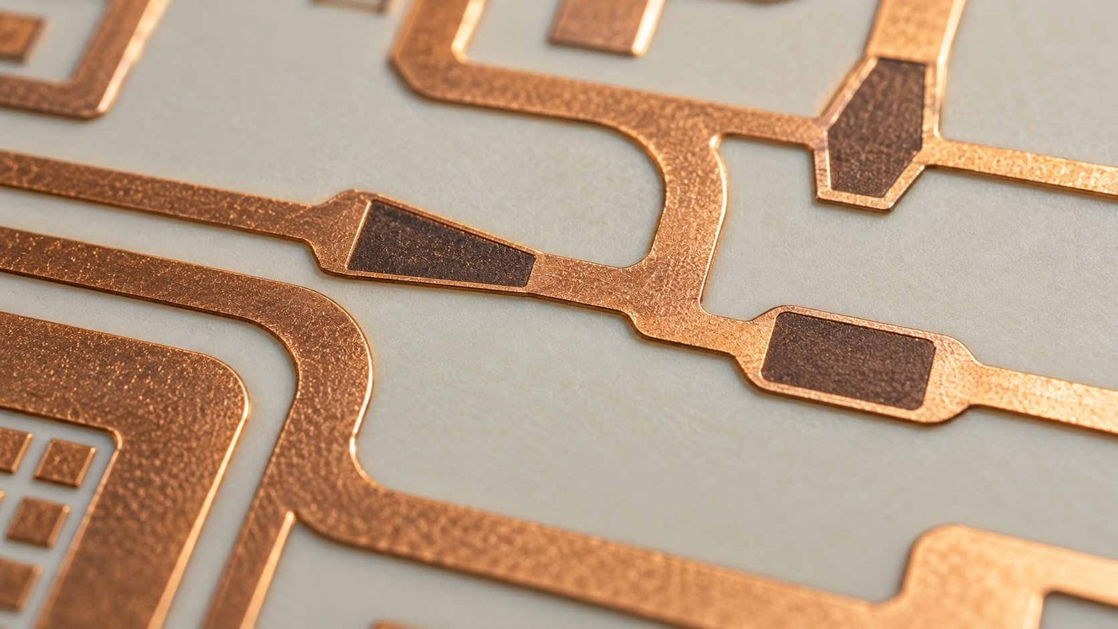
Standard π-pad arithmetic — k = 10^(3/20), Rseries = Z0(k²−1)/2k, Rshunt = Z0(k+1)/(k−1). The embedded advantage is exactness: a fractional square is etched as a trapezoid or corner-shaped region, so any value in the range of the sheet class is available in copper — the value set is no longer a catalogue. Attenuators and gain-equalizer ladders live on exactly this property.
Every discrete attenuator design has met this wall: the exact π-pad value does not exist in a catalogue series, so the design compromises to the nearest E24 value and eats the error. Etched foil dissolves the wall — fractional squares are geometry, and shaped regions (trapezoids, corner rounding) reach any value the sheet class spans. For gain equalizers and calibration-grade pads, that is the difference between a ladder that measures as designed and one that measures as compromised.
5. The Tolerance Chain: Etch, Measure, Trim
Embedded does not mean automatic. Resistance is geometry, so etching tolerance is resistance tolerance.
| 50 Ω resistor, by sheet class | Etched geometry | Resistance error from ±5 µm etch tolerance |
|---|---|---|
| 50 Ω/sq → one square | 300 × 300 µm | worst case ±3.3% · RSS ±2.4% |
| 100 Ω/sq → half a square | 200 × 100 µm | worst case ±7.5% · RSS ±5.6% — width tolerance dominates |
| Trimmed to ±1% | ±0.50 Ω at 50 Ω | Only reachable with laser trimming closed on an inline resistance probe |
R = ρ□·(L/W), so etch tolerance enters twice — once on L, once on W — and enters hardest on narrow bodies, which is precisely where high sheet resistance wants to go. The numbers above assume a ±5 µm etch tolerance, an industry-typical class (stated assumption). This is why embedded resistors change the fabricator’s metrology and not just the etch step: without a 100% inline resistance measurement feeding the trim station, a ±1% deliverable is a promise with no process behind it.
The lesson of the table is where the difficulty concentrates: tolerance enters twice — on length and width — and width dominates, which is exactly where high sheet-resistance designs go. As-etched parts are statistical (±10% class); ±1% parts are manufactured by measurement — laser trimming closed on a 100% inline resistance probe. That metrology loop is the real cost of embedding, and it separates fabricators who own the process from fabricators who own the laminate.
6. Buried Means Records: What Acceptance Rests On
A component inside the laminate cannot be inspected after the fact. Acceptance therefore moves from post-build inspection to in-process records.
| Fabrication record | What it protects in the customer’s build | Why the link is direct |
|---|---|---|
| Foil batch data — source, sheet resistance, roughness class | Amplitude accuracy of pads and equalizers, insertion-loss flatness | The resistor is the foil; the batch is the component’s data sheet |
| Etch compensation records per layer | Resistance distribution across the panel and across the lot | Etch bias is the dominant systematic error in as-etched values |
| 100% inline resistance probe + trim records | Every ±1% specified value, with serial traceability | Specified precision without a measurement record is not a spec — it is hope |
| Lamination and cleanliness records of the resistive layer | Adhesion and integrity of the buried film | A buried film cannot be inspected after lamination — the record is the inspection |
This is the manufacturing consequence of putting passives inside the laminate: the quality evidence moves from post-build inspection to in-process records, because the component is no longer reachable afterwards. Quote requests that name the foil source, sheet class, tolerance, roughness and traceability (as the briefing’s supply-chain note suggests) are therefore answerable with the process records above. Panel-level measurement method is treated in our mmWave PCB VNA testing guide.
Read top-down, the table is the acceptance plan; read bottom-up, it is the process. Either way the conclusion holds: a fabricator who ships foil batch data, etch compensation records, probe and trim data, and lamination records with the boards is delivering the only inspection a buried component will ever get.
7. The Embedded-Resistor RFQ Checklist
Eight lines, none exotic, each traceable to a number computed above.
| # | Drawing or PO line item | Why it is on the list |
|---|---|---|
| 1 | Each embedded resistor with target value, tolerance class (as-etched or trimmed) and sheet class | Tolerance class decides whether trimming metrology is in the loop (section 5) |
| 2 | Foil specification: source, sheet resistance, copper roughness class | At 28–40 GHz the foil finish is a loss spec, not a detail (section 2) |
| 3 | Amplitude-critical networks (pads, equalizers) marked as trim-required where ±1% is intended | Exact values are etched; exact tolerances are trimmed (section 4) |
| 4 | Power dissipation per resistor body with the width it implies | Resistance lives in foil — dissipation sets geometry, not vice versa (section 3) |
| 5 | Inline resistance probe coverage stated (100% vs sampling) | The trim loop and the acceptance record share the same measurement (section 6) |
| 6 | Lamination cycle and cleanliness spec for the resistive layer | A buried film is verified by records, not by post-build inspection (section 6) |
| 7 | Impedance coupon with embedded-resistor structures per panel | Batch evidence for the values shipped, not just the traces (section 6) |
| 8 | Temperature range and TCR expectation for amplitude-flat behaviour | Tens-of-ppm/°C films keep equalizers equal across the range (section 2) |
Eight lines, each tracing to a number or a mechanism above. An embedded-resistor RFQ that carries these eight answers is quotable on engineering — and auditable afterwards.
The pattern across the page: embedded resistors move quality evidence in-process and move the value set out of the catalogue. Radar and array programmes already designing for Ka band are treated in our X- and Ku-band AESA radar PCB manufacturing guide, and the low-noise chains that sit downstream of every attenuation network in the low-noise amplifier PCB design guide.
Embedded Resistor PCB — Frequently Asked Questions
How buried thin-film resistors work, why chip parts fail at mmWave, achievable values and tolerances, fabricator controls, and what the RFQ should contain.
What is an embedded resistor in a PCB?
A resistor formed inside the board instead of mounted on it. A resistive alloy film (typically NiP-type) is laminated onto the copper foil, so after etching, selected regions of the trace become resistors defined purely by geometry — length divided by width in squares of the film’s sheet resistance. No chip, no solder joints, no attachment pads. Typical published sheet-resistance classes are 25, 50 and 100 Ω/sq, with as-etched tolerances around ±10% and laser trimming available for ±1%-class values.
Why do chip resistors stop working at millimetre-wave frequencies?
A chip resistor is a series chain: pads, solder joints and the part itself, with an equivalent series inductance around 0.4 nH for a 0402 class. That reactance is 25 Ω at 10 GHz, 70 Ω at 28 GHz and 100 Ω at 40 GHz — at Ka band it exceeds the 50 Ω system impedance, so the assembly behaves mostly as an inductor. Physically, the footprint is also the same order as a quarter wavelength at 28 GHz (about 1.7 mm). An embedded resistor has no pads or joints: the resistive region is part of the transmission line.
What values can be made, and how accurate are they?
Any value in the range of the sheet class, because the value is set by geometry — a 3 dB π-pad needs 17.61 Ω series and 292.4 Ω shunt arms, and fractional squares are etched as shaped regions. As-etched accuracy is limited by etch tolerance entering both length and width: a 100 Ω/sq, 200 × 100 µm body carries ±5.6% (RSS) from a ±5 µm etch, so ±1%-class parts require laser trimming closed on an inline resistance probe.
What does the fabricator have to control that a standard build does not?
Etch compensation per layer (the dominant systematic error on values), 100% inline resistance measurement feeding the trim station, lamination cleanliness and records for a film that cannot be inspected after bonding, and foil batch traceability — source, sheet resistance and copper roughness class, which at 28–40 GHz is an insertion-loss spec. The quality evidence shifts from post-build inspection to in-process records, because the component is buried.
What should an embedded-resistor RFQ include?
Per-resistor value, tolerance class and sheet class; the foil specification with roughness class; which networks are trim-required for ±1%; power dissipation per body; inline probe coverage (100% or sampling); the lamination and cleanliness spec for the resistive layer; impedance coupons containing embedded-resistor structures per panel; and the temperature range with the TCR expectation. Suppliers who ask for these before quoting are pricing engineering, not guessing.
Designing a board with embedded thin-film resistors?
Send us the resistor schedule — values, tolerance classes, sheet class — the foil specification and the networks you intend to trim. We will review the etch compensation, the inline resistance measurement and the lamination records at process planning, and ship batch traceability, probe data and impedance coupons with the boards to IPC Class 3.
Contact Us → WhatsApp: +86 137 6047 3650Request a PCB Quote
Upload your Gerber ZIP file and project requirements. Our engineering team will review your PCB material, stackup, impedance needs, surface finish, and production quantity before quoting.
Please prepare:
- Gerber files in ZIP format
- PCB material or stackup requirements
- Controlled impedance notes if available
- Prototype or batch production quantity