Phased Array PCB Manufacturer — RO3003 Dk Uniformity, TDR ±5%

Riching PCB manufactures phased array PCB for AESA defense radar, satcom beamforming and 5G mmWave arrays. Rogers RO3003 in stock with tight Dk tolerance (±0.04) — critical for element-to-element phase consistency. TDR ±5% measured per panel. In-house plasma activation. IPC Class 3 on request. 7–10 day prototype. No MOQ.

Table of Contents

±0.04

Dk tolerance
RO3003 in stock

±5%

TDR per panel
report provided

Class 3

IPC on request
full traceability

7–10

day prototype
no MOQ

Why Dk Uniformity Matters for Phased ArraysPhased array PCB Dk uniformity diagram showing how Dk variation across panel causes beam pointing phase error

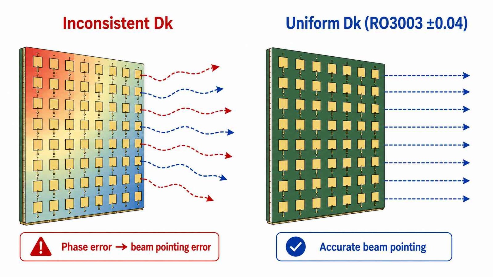
In a phased array, each antenna element’s phase is set by the feed network electrical length, which depends on the substrate Dk. If Dk varies across the panel — even slightly — elements at different positions have slightly different electrical lengths for the same physical trace length. This produces a systematic phase error across the array, which translates directly into beam pointing error.

Rogers RO3003 specifies Dk 3.0 ±0.04 — among the tightest tolerances in the PTFE material range. Combined with controlled manufacturing process (single-lot allocation, max 2 lamination cycles, TDR verification per panel), this minimizes the systematic Dk variation that causes phase error.

Manufacturing Controls for Phase Consistency

FactorWhy It MattersRiching PCB Approach
Panel-level Dk uniformityDk variation between elements causes phase error → beam pointing errorRO3003 ±0.04 Dk — tightest in PTFE range
Element-to-element impedance matchImpedance mismatch causes amplitude taper errorTDR ±5% measured per panel, report provided
Via fence consistencyInconsistent fence affects element isolation differently per element0.4mm center-to-center via spacing — uniform across panel
Lamination cycle limitRepeated press cycles shift Dk non-uniformly across panelMax 2 cycles enforced — prevents cumulative Dk drift
Material lot consistencyDifferent material lots within one array = systematic phase errorSingle-lot material allocation for multi-panel orders — on request

Applications

ApplicationTypical StackupNote
AESA defense radar (X/Ku/Ka band)RO3003 0.127 / 0.254mm, 4-8LIPC Class 3, ±5% TDR, full traceability
Satcom phased array antenna (Ka-band)RO3003 0.127mm + RT5880 hybridBondply 2929 at PTFE interfaces
5G mmWave beamforming moduleRO3003 / RT5880, 4-6LMin trace/space 2.5mil for dense routing
TR (Transmit/Receive) module arrayRO3003 0.127mm, single or dual layerBGA pads for TR chip — 0.2mm min drill
AESA feed networkRO3003 + FR4 hybridFR4 inner layers for DC distribution and control

Process Capabilities for Phased Array PCB

  • RO3003 0.127mm and 0.254mm in stock — no material procurement delay
  • TDR impedance verification per panel — ±5% tolerance available, report provided
  • Single-lot material allocation for multi-panel orders — on request
  • Min trace/space 2.5mil / 2.5mil — dense corporate feed network routing
  • Min drill 0.2mm mechanical, 0.1mm laser — BGA pads for TR module ICs
  • Via fence: 0.4mm center-to-center — uniform element isolation
  • Max 2 lamination cycles — prevents cumulative Dk drift across panel
  • Hybrid RO3003 + FR4 stackups — Rogers 2929 bondply for DC/control layer integration
  • IPC Class 3 on request — full material traceability and lot documentation

How to Order

  • WhatsApp: +86 13760473650
  • Send: Gerber zip + NC drill + stackup drawing
  • Specify: RO3003 thickness, impedance tolerance (±5% recommended), IPC Class, panel quantity
  • Note if single-lot material allocation is required for multi-panel arrays
  • DFM review: 4–8 hours

Phased Array PCB Manufacturer — Shenzhen Direct Factory

RO3003 In Stock · ±0.04 Dk Tolerance
TDR ±5% Per Panel · IPC Class 3 · No MOQ

Send Gerber + stackup drawing. DFM review within 4–8 hours.
Specify panel quantity and single-lot allocation if required.

WhatsApp +86 13760473650

DFM review within 4–8 hours

PCB Project Review

Request a PCB Quote

Upload your Gerber ZIP file and project requirements. Our engineering team will review your PCB material, stackup, impedance needs, surface finish, and production quantity before quoting.

Please prepare:

  • Gerber files in ZIP format
  • PCB material or stackup requirements
  • Controlled impedance notes if available
  • Prototype or batch production quantity
ZIP format only. Please compress all Gerber and drill files into one ZIP package before uploading.