
250 GHz Characterization Boards: Differential Probe Pads, Thermal Imaging and the Cold-to-Hot Account
250 GHz characterization board design: differential probe pad geometry, calibration planes, 50 ns thermal imaging and the expansion account from −60 to +300 °C.
Home » 250 GHz Characterization » 250 GHz Characterization Boards: Differential Probe Pads, Thermal Imaging and the Cold-to-Hot Account
Table of Contents
A probe station that can sweep DC to 250 GHz in a single pass changes what a characterization board has to be. When the quarter wavelength is 300 µm and a pad is 100 µm wide, the pad is not a contact — it is a circuit element. And when the same platform also images a hotspot with 50 ns pulses, the surface of that pad stops being cosmetic and becomes part of the measurement.
Two disciplines that are usually separated now have to agree on one piece of copper. The RF side cares about symmetry, reference plane and de-embedding; the thermal side cares about finish, flatness and a known dissipating element. A board that satisfies one and not the other produces data that is internally consistent and externally wrong.
The S-parameter method at lower millimetre-wave frequencies is set out in our mmWave VNA testing guide and the calibration-board geometry in the 110–145 GHz calibration board work. This page is about what changes when the probe is differential and the frequency reaches 250 GHz.
1. When the Pad Is Bigger Than a Quarter Wavelength
There is a frequency above which the phrase "test pad" stops being accurate, and 250 GHz is comfortably past it.
| Frequency | λ0 in air | λ0/4 | Gold skin depth | A 100 µm pad is |
|---|---|---|---|---|
| 100 GHz | 2.998 mm | 749.5 µm | 0.2486 µm | 3.3% of a wavelength |
| 150 GHz | 1.999 mm | 499.7 µm | 0.2030 µm | 5.0% |
| 200 GHz | 1.499 mm | 374.7 µm | 0.1758 µm | 6.7% |
| 250 GHz | 1.199 mm | 299.8 µm | 0.1572 µm | 8.3% |
A quarter wavelength at 250 GHz is 300 µm — smaller than the probe's own contact geometry. There is no part of this board that behaves as a lumped element.
The consequence is that the footprint has to be designed the way a launch is designed: pad size set for the probe's contact geometry, return vias placed for the current path rather than for convenience, and the transition from pad to line treated as a discontinuity to be matched. A footprint copied from a 67 GHz design will work, in the sense that contact is made — and will carry an impedance discontinuity that is invisible in the DC test and dominant in the S-parameter data.
2. Differential Means Symmetry Is Mandatory
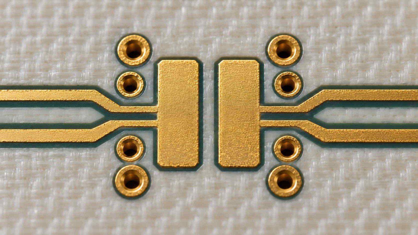
A differential probe measures two legs against each other, and its calibration assumes the two legs see the same environment. That assumption is a property of the board, not of the instrument.
| Symmetry error between the two legs | Effect at 250 GHz | Detectable in |
|---|---|---|
| 5 µm length difference | Phase error of several degrees at λg/4 scale | Differential S-parameters |
| 0.5 dB amplitude difference | Mode conversion into the common mode | Common-mode rejection measurement |
| One leg with an extra ground via | Different return inductance per leg | Visible only as unexplained calibration residual |
| Asymmetric mask opening | Different reference plane per leg | Cross-section, then S-parameters |
Symmetry is a geometric property of the pad pair and its return vias, so it is decided at the footprint — a differential probe cannot calibrate away a difference in its own two legs.
The failure mode is quiet. One leg with an extra ground via, or one leg whose mask opening is 15 µm wider, produces a return-inductance difference between the legs. The measurement still returns numbers, they are still repeatable, and they contain a mode-conversion term that belongs to the board. Nothing in the setup flags it, because the calibration was performed on a symmetric standard and the board is not symmetric.
Which is why the first article for a differential characterization board should include a cross-section through the pad pair. It is the only direct evidence that the two legs are the same structure, and it is cheap compared with the cost of discovering the asymmetry through an unexplained offset in device data six months later. The same principle governs symmetric launch design in our RF connector launch guide.
3. Calibration Removes the Probe, Not the Board
The single-pass differential measurement that these platforms offer includes a correction for crosstalk between the two probes. That correction is a model of the probe pair, and like every model it has a reference plane.
| Coupon element | What it proves | Why it cannot be omitted |
|---|---|---|
| Differential through line at the design pitch | Impedance and loss of the intended geometry | A single-ended coupon proves a different board |
| Differential open and short | Reference plane definition | Without them the de-embedding is an assumption |
| Symmetric pad pair with matched return vias | Mode purity | The probe cannot correct its own leg mismatch |
| Thermal test structure with a known dissipating element | The thermal imaging is calibrated | A hotspot image with no known source is a picture, not a measurement |
| Cross-section through the pad pair | Mask, finish, plating | The only direct evidence of the reference plane |
Five elements. The second is the one that is usually improvised, and it is the one that decides whether the reported number belongs to the board or to the setup.
The practical rule is that the reference plane has to be defined before the coupon is designed, because it decides which structures the coupon needs. If the reported number is at the probe tips, the de-embedding is short and the coupon is dominated by open and short standards at the real pitch. If the reported number is at the device, the coupon has to carry the full transition — and then the coupon is effectively a second board that must itself be characterised.
The failure that follows from skipping this is familiar: a coupon that measures beautifully and a device measurement that does not match it, with no way to attribute the difference. The fixture side of the same problem is treated in our RF and mmWave test fixture guide.
4. Thermal and Electrical at the Same Time
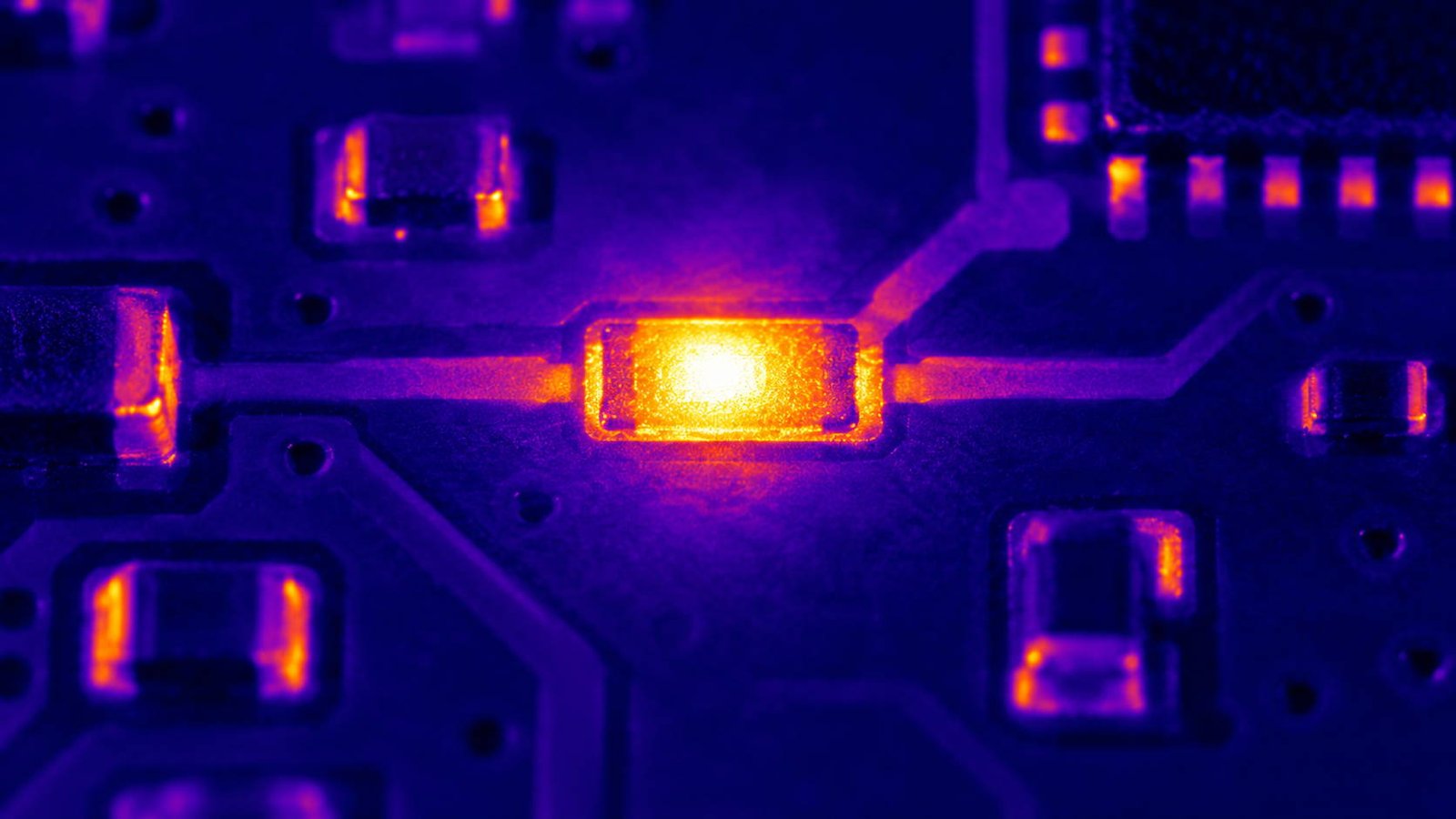
Simultaneous thermal imaging turns a separate experiment into a correlated one: the electrical behaviour and the local hotspot are observed at the same bias. The resolution of that observation is set by the pulse width, and the relationship is not linear.
| Pulse width | Thermal diffusion length in copper | What it resolves | Board consequence |
|---|---|---|---|
| 50 ns | 2.42 µm | The surface layer of the pad and the first few microns of copper | Pad surface finish and flatness dominate the image |
| 5 ns | 0.765 µm | The metal stack, still not the dielectric | Layer boundaries become visible |
| 500 ps | 0.242 µm | A surface skin of metal only | Any roughness or residue appears as an artefact |
Diffusion length is √(α·t) with α = 1.17e-4 m²/s for copper. Short pulses measure the surface, so the surface has to be worth measuring — which is a fabrication requirement, not a measurement one.
At 50 ns the image is a surface measurement of a few microns of copper. That is genuinely useful for locating a hotspot at a junction or a bond, and it is also a warning: whatever is on the surface — finish roughness, residue, a scratch — will appear in the image. A pad that would be acceptable for RF alone can produce a thermal artefact, and the fix is fabrication rather than measurement.
The board requirement that follows is unglamorous and decisive: a controlled, consistent surface. Finish thickness within specification, no residue, flatness within the probe's compliance. Those are the same requirements that make the RF contact repeatable, which is convenient — the two disciplines agree on the surface and disagree only about what they are measuring there.
5. The Cold-to-Hot Account
A platform that spans −60 to +300 °C puts every dimension on the board through a 360 K excursion. The arithmetic is worth doing, not because the numbers are large, but because they are the same size as the tolerances being claimed.
| Dimension | Expansion over −60 to +300 °C | Significance |
|---|---|---|
| 0.3 mm probe pitch | 1.84 µm | Under 1% of the pitch — the probe compliance absorbs it |
| 0.5 mm pitch | 3.06 µm | Still small, but the probe's own expansion now matters too |
| 1.0 mm pitch | 6.12 µm | Comparable to a typical contact compliance budget |
| Reference: gold skin depth at 250 GHz | 0.1572 µm | Two orders smaller — this is why finish thickness is quoted in tenths of a micron |
Expansion of the laminate at 17 ppm/K over a 360 K span, calculated on the pitch. The point is not that the numbers are large — they are not — but that they are the same order as the geometric tolerances being claimed.
On a 0.3 mm pitch the expansion is under 1% and the probe's compliance absorbs it without difficulty. On a 1.0 mm pitch it approaches the compliance budget, and the probe's own expansion becomes part of the problem rather than a margin. Neither is a crisis — but a specification that quotes a pitch to a micron and ignores a 6 µm excursion is quoting a number that only holds at one temperature.
For the material side, the relevant question is dimensional stability rather than loss, and the available laminate families differ substantially in how they behave over that range. The selection criteria are collected in our high-frequency PCB materials section, and the coefficient-of-expansion consequences for plated structures in the high-frequency drilling capabilities guide.
6. What the Coupon Has to Contain
Everything above reduces to a list of structures that must exist on the coupon, and the list is short enough that there is no excuse for omitting any of it.
A differential through line at the design pitch gives impedance and loss for the intended geometry. Differential open and short structures define the reference plane, without which the de-embedding is an assumption rather than a calculation. A symmetric pad pair with matched return vias is the mode-purity check. A thermal structure with a known dissipating element turns a hotspot image into a calibrated measurement. And a cross-section through the pad pair is the only direct evidence that the mask, the finish and the plating are what the drawing said.
The order matters as much as the list: open and short measured before the device, thermal structure characterised before the device is biased. Each step removes an unknown that would otherwise be attributed to the device. That discipline is what separates a characterization board from a test vehicle with a nice photograph attached.
7. The 250 GHz Characterization Board RFQ Checklist
Related reading
- W-band noise figure measurement on PCB — Y-factor arithmetic, source match uncertainty and the finish that decides 75–110 GHz
- 1 mm switch-connector RF test point DFM — pad geometry, ground-return inductance and probe keep-out at 15 GHz
- mmWave PCB VNA testing — S-parameter measurement, calibration and de-embedding
- mmWave test fixture PCB design — fixture launch, grounding and repeatability
Eight lines. The third and the seventh are the two that turn a measurement into a claim.
| # | Item to specify | Why it decides the outcome |
|---|---|---|
| 1 | Maximum measurement frequency | Sets λ0/4 — the scale against which every feature is judged |
| 2 | Probe type, pitch and compliance | The pad geometry has to match the probe, not the reverse |
| 3 | Single-ended or differential | Differential makes symmetry a hard geometric requirement |
| 4 | Temperature range | Sets the expansion account and the material choice |
| 5 | Whether thermal data is required simultaneously | Decides the finish and the surface quality |
| 6 | Calibration structures to be included on the coupon | Open, short, through and load at the real pitch |
| 7 | De-embedding reference plane | The number being reported is defined relative to it |
| 8 | Evidence package | Cross-section, coupon S-parameters, calibration residual |
Eight lines. Lines 3 and 7 are the two that turn a measurement into a claim.
The pattern: a 250 GHz characterization board is specified by symmetry and reference plane, and proved by a coupon that carries the real geometry plus a cross-section that shows it. The probe is calibrated; the board has to be correct.
250 GHz Characterization Board — Frequently Asked Questions
Probe pad geometry at 250 GHz, differential symmetry, calibration reference planes, 50 ns thermal imaging and what expansion over −60 to +300 °C really means.
Why is 250 GHz a different problem from 110 GHz?
Because the quarter wavelength falls to 300 µm, which is smaller than the contact geometry of the probe itself. At 110 GHz a quarter wavelength is 681 µm and a pad can still be treated as a small feature; at 250 GHz a 100 µm pad is 8.3% of the free-space wavelength, so the pad, its return vias and the probe tip form a distributed network. Every dimension of the footprint becomes an electrical parameter.
Does differential probing really require a symmetric footprint?
Yes, and it is the one part of the error budget the probe cannot correct. Calibration removes the probe's own systematic behaviour, but it assumes the two legs see the same thing. If the pad pair gives one leg an extra ground via or a different mask opening, the two legs have different return inductance and the calibration residual turns into an unexplained offset. Symmetry is decided in the footprint, so it has to be checked there.
What does a 50 ns thermal pulse actually measure?
A surface layer about 2.4 µm deep. Thermal diffusion length is √(α·t), and for copper over 50 ns that is a few microns — so the image is dominated by the pad's finish, its flatness and the first layers of plating, not by the dielectric below. That is a useful measurement, but it makes surface quality a prerequisite: a rough or residue-covered pad produces an artefact that looks like a hotspot.
Is thermal expansion a real problem over −60 to +300 °C?
On a 0.3 mm pitch, no — the drift is 1.84 µm, well inside a probe's compliance. The reason to compute it anyway is that it is the same order as the geometric tolerances being claimed elsewhere on the board: the gold layer is 0.050 µm thick and the skin depth at 250 GHz is 0.1572 µm. When expansion, finish and tolerance are all single-digit microns, a specification that quotes tenths has to say which one it means.
Can a board supplier provide a 250 GHz coupon without owning a 250 GHz setup?
Yes — the coupon is a board, and the measurement is a service. What the supplier must own is the geometric accuracy: pad position, symmetry of the pair and its return vias, mask registration, finish thickness and flatness. Those are all measurable optically and by cross-section. The 250 GHz measurement then confirms what the geometry promised, which is why the coupon has to carry the real geometry rather than a proxy.
What is the most common defect on a characterization board?
An asymmetric return path under a differential pad, and an uncontrolled reference plane between the coupon and the probe. Both are invisible in continuity test and both produce results that look like device behaviour. The defence is a cross-section through the pad pair on the first article, and a coupon whose open and short structures are measured before the device is.
Building a characterization board for 250 GHz probing?
Send the probe type and pitch, the frequency range, the temperature range and whether you need simultaneous thermal data. We will size the pad pair for symmetry, place the return vias, set the finish and flatness for the imaging requirement, include the calibration structures at the real pitch, and ship the evidence package — cross-section, coupon S-parameters and pad-position Cpk — with the boards to IPC Class 3.
Contact Us → WhatsApp: +86 137 6047 3650Request a PCB Quote
Upload your Gerber ZIP file and project requirements. Our engineering team will review your PCB material, stackup, impedance needs, surface finish, and production quantity before quoting.
Please prepare:
- Gerber files in ZIP format
- PCB material or stackup requirements
- Controlled impedance notes if available
- Prototype or batch production quantity