
RF Test Point DFM: Making a 1 mm Switch Connector Footprint Work to 15 GHz
RF test point PCB design for 1 mm switch connectors to 15 GHz: pad geometry, ground-return inductance, probe keep-out and panel-to-panel loss consistency.
Home » High Density PCB » RF Test Point DFM: Making a 1 mm Switch Connector Footprint Work to 15 GHz
Table of Contents
A switch connector is the least glamorous component on a high-frequency board and one of the few that the end user touches. It exists so that a probe can reach a node during test and so that the node is a clean 50 Ω line the rest of the time. Making it a millimetre square and taking it to 15 GHz does not change that job — it changes how much of the layout the job consumes.
The arithmetic is short. At 15 GHz a free-space wavelength is 19.99 mm, so a 1.0 mm footprint is 5.0% of a wavelength rather than a point. Half a nanohenry of ground-return inductance is 47 Ω of reactance at the same frequency — as large as the signal impedance it is supposed to reference. And the area needed to reach the connector with a probe barely follows the connector's own shrinkage: the body fell 40%, the occupied area fell 60% only because the probe got smaller too.
This page is about the footprint and the process around it. The transition from a connector into a trace — the launch itself — is covered in our RF connector launch guide, and the vertical, solderless case in the board-to-board RF connector guide.
1. At What Frequency Does a Test Point Stop Being a Point?
The usual rule of thumb is that a structure is lumped while it is smaller than a tenth of a wavelength. Applied to a 1 mm footprint, that rule puts the boundary at about 10 GHz and declares everything above it a distributed problem.
| Frequency | λ0 in air | λ0/10 | 1.0 mm footprint as a fraction of λ0 | Is it lumped? |
|---|---|---|---|---|
| 1 GHz | 299.79 mm | 29.98 mm | 2.0% | Yes — geometry barely matters |
| 6 GHz | 49.97 mm | 5.00 mm | 2.0% | Yes |
| 10 GHz | 29.98 mm | 3.00 mm | 3.3% | Borderline |
| 15 GHz | 19.99 mm | 2.00 mm | 5.0% | No — the footprint is a distributed structure |
The same 1 mm footprint is invisible at 2 GHz and dominant at 15 GHz. Nothing about the connector changes; only the wavelength around it does.
The rule is crude but the conclusion is right. Between 10 and 15 GHz the pad, the mask opening and the ground vias stop acting as a single node and start acting as a short transmission line with two discontinuities. That does not make the part unusable — the connector is specified to 15 GHz — it means the footprint is now part of the electrical design and has to be reviewed as such, rather than copied from a land pattern.
2. The Switch Contact Cuts Both Ways
A switch connector contains a moving contact that opens when a probe is inserted and closes when it is withdrawn. Electrically that is two different networks, and both have to be acceptable: the closed state has to look like a through-connection with a defined impedance, and the open state has to isolate well enough that the node is not loaded by a stub during normal operation.
The closed state gets the attention because that is when a measurement is being made. The open state is the one that runs for the life of the product, and it is where a poorly designed footprint does its damage quietly: a switch that closes onto a pad with excessive return inductance leaves a small residual reactance in the signal path permanently. Nothing in a functional test reveals it, because the product still works — it simply works with a slightly worse match than the design assumed.
The contact also wears. Every insertion removes a little material, and the finish that survives thousands of cycles at a fraction of a skin depth is not necessarily the finish that survives them mechanically. The two requirements — electrical adequacy and wear resistance — point at different thicknesses, and the thicker of the two wins because only one of them degrades over time.
3. Ground Return: The Parasitic That Decides Everything
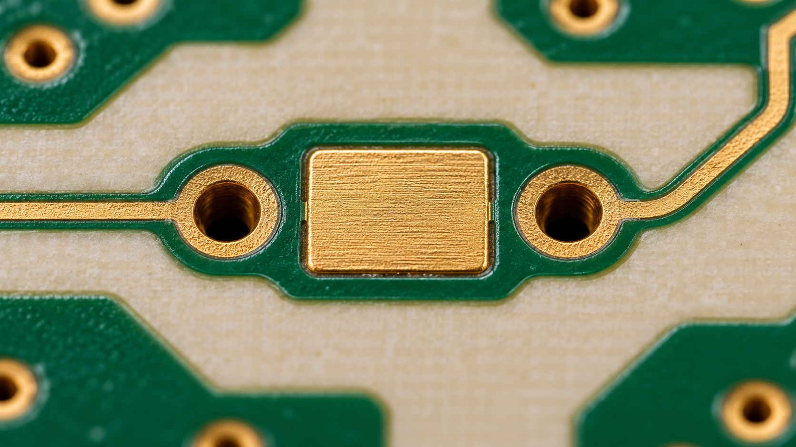
Signal paths get designed; return paths get inherited. At a test point the return path is two or three vias and the distance from the pad edge to them, and at 15 GHz that distance is an inductance large enough to matter on its own terms.
| Parasitic | Reactance at 15 GHz | Compared with 50 Ω | Where it comes from |
|---|---|---|---|
| 0.3 nH | 28.3 Ω | 57% of the signal impedance | A single short ground via adjacent to the pad |
| 0.5 nH | 47.1 Ω | 94% | One ground via, one mask opening, one 0.5 mm return path |
| 0.8 nH | 75.4 Ω | 151% | A return path that shares vias with the digital ground |
Series reactance of this magnitude in the ground return is not a refinement — it is the difference between a 50 Ω test point and an unmatched stub.
The useful way to read the table is to compare each reactance with 50 Ω. At 0.3 nH the return is a fifth of the signal impedance — a perturbation worth knowing about. At 0.5 nH it is essentially equal to the signal impedance, which means the return path is no longer a reference; it is a second element in series with the signal. At 0.8 nH the test point has become a filter.
The layout rule that follows is not subtle: two ground vias immediately beside the pad, connected to the ground plane with no shared barrel, and no thermal-relief spokes in the path. The same principle governs the via patterns around launch structures, covered in our via design for RF guide, and the ground-plane continuity question in the controlled impedance guide.
4. The Area the Datasheet Does Not Draw
A connector body of 1.0 × 1.0 × 0.55 mm is a fact. What the layout needs is the area in which nothing else may be placed, and that is set by the probe: its approach angle, its compliance travel and the clearance the operator needs around it.
| Quantity | Value | Derived from |
|---|---|---|
| Footprint area, current generation | 1.0 mm² | 1.0 × 1.0 mm body |
| Footprint area, previous generation | 1.667 mm² | 40% reduction stated for the new part → 1.29 mm square equivalent |
| Occupied area including probe keep-out, current | 1.0 mm² | Same, when the probe is not considered |
| Occupied area including probe keep-out, previous | 2.50 mm² | 60%% reduction stated when the keep-out is counted |
The difference between the first and last row is the whole story of high-density RF test: the component shrank, but the space needed to reach it barely did.
This distinction matters most in the products that drove the miniaturisation — wearables, hearables, dense phone boards — because those are exactly the layouts where a keep-out that is 60% larger than expected breaks the floorplan. The published figures are 40% for the footprint and 60% when the probe keep-out is counted, and the second number is the honest one for planning purposes.
There is a second-order cost as well. A small pad on a tight pitch means the mask opening is small, and mask registration tolerance does not scale with the pad. On a 0.25 mm pad, a 25 µm registration error is 10% of the feature; on a 1 mm pad it is 2.5%. So the same process capability that was comfortable on the previous generation becomes marginal on this one, and the DFM review has to say so before the mask is ordered. Related process limits are in our high-frequency DFM review guide.
5. Six DFM Items, One of Which Is Not Negotiable
A test point footprint is small enough that a review can be a checklist rather than a project. The items below are the ones that actually move the measurement.
| DFM item | Target | Consequence of missing it |
|---|---|---|
| Pad size and shape | Matched to the probe tip, not to the land pattern alone | Contact resistance varies with placement |
| Solder mask opening | Annular, with a controlled dam | Mask encroachment shifts the reference plane |
| Pad-to-ground via distance | As short as the keep-out allows | 0.5 nH of return inductance = 47.1 Ω at 15 GHz |
| Coplanarity across the pad pair | Within the probe's compliance | One contact lifts, loss jumps |
| Placement accuracy | Cpk ≥ 1.33 on pad centre | Probe alignment drifts across a panel |
| Finish | Gold thick enough for repeated contact | Contact resistance rises with every insertion |
Six items, all of them decided at the footprint and the finish, none of them recoverable by test.
The non-negotiable one is the via distance. Everything else on the list has a tolerance band within which the result is acceptable; the return inductance is a first-order term at 15 GHz and there is no compensation for it later. If the keep-out forces a compromise, give up pad area before giving up via proximity.
Second in importance is the finish, but for a reason that is mechanical rather than electrical. At 15 GHz the skin depth in gold is 0.642 µm, so a thin gold is already electrically sufficient; what it is not is durable. A test point that sees thousands of insertions needs enough gold to wear, and that number comes from the product life rather than from the frequency.
6. Consistency Across a Panel, Not Just Compliance
A single test point that measures correctly proves very little. The failure mode that matters is drift: etch and mask registration moving together across a panel or between lots, so that some boards have a test point that is 0.1 dB worse than the coupon said. No continuity test sees it, and no functional test fails — the board simply has less margin than the design assumed.
| Metric | Sampling | Why it is the one to watch |
|---|---|---|
| Insertion loss per test point | One per panel, coupon | Catches drift in etch and mask registration together |
| Contact resistance after N insertions | First article, then per lot | The switch contact wears; the pad must not |
| Pad centre position | Cpk per panel | Directly converts to probe alignment error |
| Finish thickness | Per lot certificate | Sets contact life and, above 10 GHz, loss |
| Voiding under the pad | Cross-section, first article | A void is both a thermal and a return-path defect |
Five metrics. The first is the only one that measures the electrical result directly; the rest explain it when it moves.
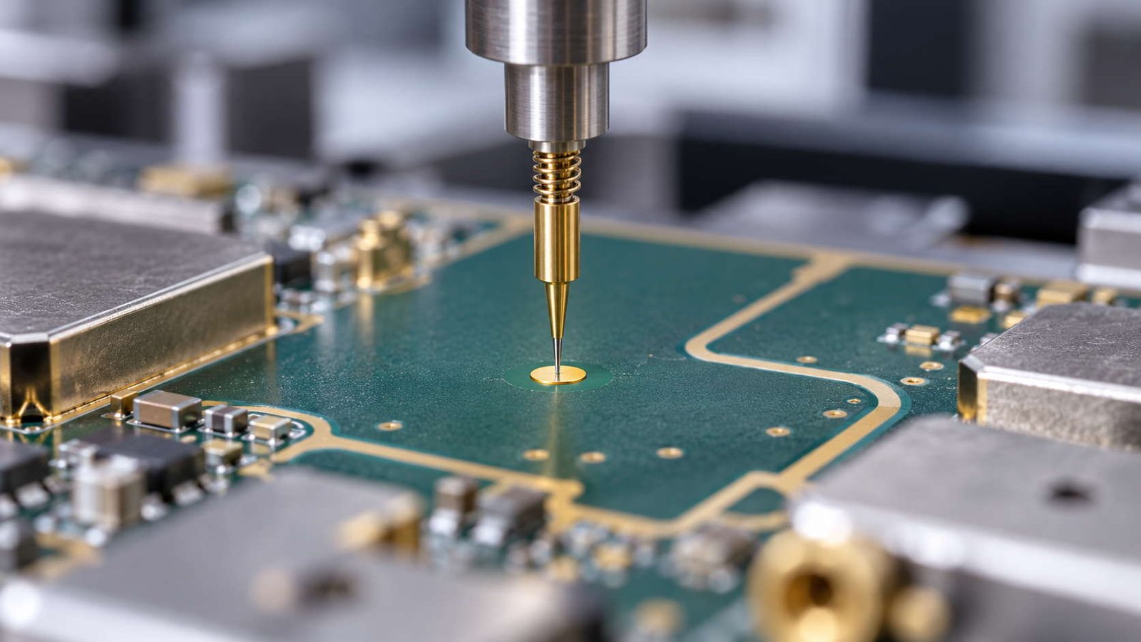
This is why insertion loss per panel on a coupon that carries the real footprint is the metric to insist on. It is the only one that measures the electrical consequence directly; the others explain the result when it moves. The general framework for this kind of inspection is in our RF PCB quality control guide, and the finish options in the RF surface finish guide.
7. The RF Test Point RFQ Checklist
Related reading
- 60 GHz dual-beam communication module PCB — element pitch, beam-to-beam isolation and the 57–70 GHz loss budget
- 77 GHz radar SoC PCB design for 4T4R — virtual-array pitch, the phase budget in degrees per millimetre, and Dk batch tolerance
- RF connector launch design — the transition from coax to planar line
- high-frequency PCB DFM review — the checks that catch a build before the panel is cut
Eight lines, and the second one is the one that changes the layout.
| # | Item to specify | Why it decides the outcome |
|---|---|---|
| 1 | Connector part number and its frequency limit | The limit is where the footprint stops being lumped |
| 2 | Probe type and its keep-out envelope | Sets the real occupied area, not the body size |
| 3 | Test frequency and the loss budget per test point | Turns the footprint into an impedance problem |
| 4 | Number of insertions over product life | Decides the finish and its thickness |
| 5 | Ground-return topology | The single largest parasitic at 15 GHz |
| 6 | Panel quantity and the sampling plan | Decides whether consistency is proved or assumed |
| 7 | Assembly: reflow profile and mask strategy | Mask encroachment moves the reference plane |
| 8 | Evidence package | Loss per panel, Cpk, cross-section |
Eight lines. Line 2 is the one that changes the layout, and the one most often left to the mechanical team.
The pattern: a miniature test point is specified by its keep-out and its return path, and proved by per-panel loss on a coupon that carries the real footprint. The connector shrank; the discipline around it did not.
RF Test Point PCB — Frequently Asked Questions
Footprint reactance at 15 GHz, acceptable ground inductance, real occupied area with the probe keep-out, finish choice for repeated probing and how to prove panel consistency.
Why does a 1 mm connector need a DFM review at all?
Because at 15 GHz the footprint is 5.0% of a wavelength, which is no longer small compared with the signal. The pad, the mask opening and the ground-return vias together form a distributed structure whose reactance is a significant fraction of 50 Ω. At 2 GHz the same footprint is invisible; at 15 GHz it is the dominant parasitic in the test path.
How much ground inductance is acceptable at a test point?
Treat it as a fraction of the signal impedance. 0.3 nH is 28 Ω at 15 GHz, about 57% of 50 Ω — tolerable. 0.5 nH is 47 Ω, close to the signal impedance itself, and that is where the test point stops behaving like a test point. In practice this means two ground vias immediately beside the pad, not one shared with the surrounding ground pour.
The datasheet says 40% less board area. Does the layout actually shrink that much?
Only if you count the body alone. The published figures distinguish between the connector footprint — 1.0 mm² against 1.67 mm² for the previous generation — and the occupied area once the probe's operating keep-out is included, where the reduction is closer to 60%. The number that governs the layout is the second one, and it depends on the probe, not on the connector.
What finish should a test point that gets probed thousands of times use?
One with enough gold to survive repeated contact and enough thickness consistency to keep the loss stable. At 15 GHz the skin depth in gold is 0.642 µm, so the finish is electrically adequate at a fraction of a micron — the requirement here is mechanical wear rather than skin depth. That is the opposite of the situation at low frequency, where a thin gold over nickel lets the current reach the nickel.
Should the test point share ground vias with the rest of the board?
No. A shared via couples the test point's return path to whatever else uses that via, and the coupling is frequency-dependent. The test point's ground should be a local pair of vias directly beside the pad, tied into the ground plane at the shortest possible distance — the same discipline that governs launch structures, described in our RF connector launch guide.
How is consistency across a panel proved?
By measuring insertion loss per panel on a coupon that carries the real footprint, and by controlling pad position with a Cpk rather than a tolerance. Etch and mask registration drift together, so a coupon measured per panel catches both before the panel ship — which matters because the failure mode is a gradual loss increase that no continuity test will see.
Putting a 1 mm switch connector on a dense RF board?
Send the connector part number, the probe type and its keep-out envelope, the test frequency and the loss budget per test point. We will size the pad and the mask opening, place the ground-return vias, set the finish against insertion count, and ship the first-article package — loss per panel, pad position Cpk, contact-resistance report and cross-section — with the boards to IPC Class 3.
Contact Us → WhatsApp: +86 137 6047 3650Request a PCB Quote
Upload your Gerber ZIP file and project requirements. Our engineering team will review your PCB material, stackup, impedance needs, surface finish, and production quantity before quoting.
Please prepare:
- Gerber files in ZIP format
- PCB material or stackup requirements
- Controlled impedance notes if available
- Prototype or batch production quantity