
57–70 GHz Connectivity Module PCB: Two Beams, Eight Channels and a Wideband Loss Budget
60 GHz communication module PCB design for 57–70 GHz dual-beam links: element pitch, phase per millimetre, beam isolation and the wideband loss budget.
Home » 5G FWA PCB » 57–70 GHz Connectivity Module PCB: Two Beams, Eight Channels and a Wideband Loss Budget
Table of Contents
A 57–70 GHz connectivity platform is a different board problem from a radar at the same frequency. It carries data, so what matters is absolute loss and how well eight channels hold their relative phase and amplitude — not chirp linearity or range resolution. The band is 20.5% wide, the element pitch has to be chosen rather than derived, and two simultaneous beams mean the layout has to isolate them without the help of time multiplexing.
The numbers that decide it are ordinary: 3.208 mm of guided wavelength at 60 GHz, 112.2 degrees per millimetre, an 11.25° phase-shifter step that corresponds to 0.100 mm of trace, and about 12.2% of link range lost per decibel of feed loss. None of them are hard to compute. All of them are easy to lose in a layout review that treats the feed as routing.
For the sensing case at the same frequency — where the questions are range resolution and detection — our 60 GHz in-cabin radar PCB guide is the right reference. For the array-level view, see the phased array PCB guide, and for the 5G context the 5G mmWave PCB section.
1. What the 57–70 GHz Band Actually Demands
A band that spans 13 GHz of instantaneous width is not a narrowband design with margin. Everything that depends on wavelength moves with frequency, and it moves by 18.6% from one edge to the other.
| Frequency | λ0 in air | λ0/2 element pitch | Guided wavelength | Phase per mm |
|---|---|---|---|---|
| 57 GHz | 5.260 mm | 2.630 mm | 3.377 mm | 106.6° |
| 60 GHz | 4.997 mm | 2.498 mm | 3.208 mm | 112.2° |
| 66 GHz | 4.542 mm | 2.271 mm | 2.916 mm | 123.4° |
| 70 GHz | 4.283 mm | 2.141 mm | 2.750 mm | 130.9° |
0.127 mm laminate, Dk 3.00, 50 Ω microstrip (εeff = 2.426). The element pitch moves 18.6% across the band, so a fixed array is a compromise that has to be declared.
| Quantity | Value | Why it matters on the board |
|---|---|---|
| Fractional bandwidth | 57–70 GHz = 20.5% | A single feed network must hold impedance, not just loss, across it |
| λ0 variation across band | 5.260 → 4.283 mm (18.6%) | Array spacing optimised at 60 GHz is off at both ends |
| Guided wavelength at 60 GHz | 3.208 mm | Sets every length tolerance on the feed |
| Phase sensitivity at 60 GHz | 112.2°/mm | Microns become beam-pointing error |
| 5-bit phase shifter LSB | 11.25° | = 0.100 mm of line — the resolution floor of the whole chain |
| Eight-channel aperture | 19.99 mm | Mechanical span the enclosure must accommodate |
| Beamwidth, 8 elements at λ/2 | 12.7° | Coupled with pointing error, this sets scan loss |
Derived from the band edges and the laminate, not from a datasheet table.
The practical consequence is that a single feed network has to hold two different things at once. Impedance has to stay near 50 Ω across the band, which is mostly a stackup and geometry question, and the phase relationship between channels has to stay defined, which is a length question. A design optimised only at 60 GHz will be acceptable there and progressively worse at both edges — and because the platform advertises operation across the whole band, that degradation is a specification failure rather than a design margin issue.
2. Two Beams: Isolation Is a Layout Property
Two independent beams from one aperture is a scheduling idea that becomes a physical constraint. Each beam is formed by the same eight channels with a different phase set, so the isolation between the beams is not a property of the chip — it is a property of how much of each channel's signal leaks into the other beam's phase state, and that leakage is set by amplitude and phase match across the array.
| Parameter | Target | How it is proved | Failure mode if missed |
|---|---|---|---|
| Channel-to-channel amplitude | ≤ 0.5 dB | Per-channel insertion loss on a coupon | Beam squint and raised sidelobes |
| Channel-to-channel phase | ≤ 11.25° (one LSB) | Per-channel electrical length report | Pointing error that calibration cannot remove |
| Cross-polarisation isolation | ≥ 20 dB | Two-port measurement through each polarisation | Polarisation diversity degrades to a lossy single stream |
| Beam-to-beam isolation | ≥ 20 dB | Pattern measurement at the scan extremes | One beam steals gain from the other |
| Impedance, all eight ports | 50 Ω ±5% | TDR or coupon per panel | Return loss eats the margin the link budget needs |
Targets are stated as engineering goals, not as device specifications; the measurement column is what a board supplier can actually commit to.
This is why an amplitude mismatch is worse here than in a single-beam design. In one beam, a 1 dB channel error raises a sidelobe. In two beams, the same error means the two phase sets are no longer orthogonal in practice, and each beam carries a copy of the other at a level set by the mismatch — which is exactly the interference the dual-beam architecture was supposed to avoid.
Cross-polarisation isolation belongs to the same family of problems. Twenty decibels of isolation between the two polarisations on one element does not produce twenty decibels in the array, because the feed network's own asymmetry adds a common-mode term that no element design can remove. That asymmetry is a board property: a difference in via count under the two feeds, or a difference in how far each feed runs beside a ground pour edge. The array-level treatment is in the phased array PCB design guide.
3. Phase Arithmetic: 0.1 mm Is One Shifter Step
At 60 GHz on 0.127 mm laminate the guided wavelength is 3.208 mm, which gives 112.2° per millimetre of trace. Put those two numbers against a 5-bit phase shifter's 11.25° least significant bit and the result is uncomfortable: 0.100 mm of length is exactly one resolution step.
| Error source | Magnitude | Phase at 60 GHz | Beams affected |
|---|---|---|---|
| Trace length difference | 0.1 mm | 11.22° | Both — the beam moves, it does not split |
| Trace length difference | 0.05 mm | 5.61° | Marginal against an 11.25° LSB |
| Laminate Dk, batch shift | ±0.04 | 13.08° over 20 mm | Both, asymmetrically |
| Via stub in the feed | one uncontrolled stub | not computable without geometry | Shows as a null, not a bias |
The first two rows are the same error at different scales; the third is the one that cannot be corrected after lamination, because it is distributed through the whole run.
A board that is off by a tenth of a millimetre between two channels has, in effect, moved the beam by one increment on its own. That is not catastrophic — calibration can subtract a fixed offset — but only if the offset is fixed. If the error varies with frequency, which it does when the cause is distributed Dk rather than a discrete length difference, then a single calibration constant cannot remove it, and the error reappears at the band edges as pointing drift.
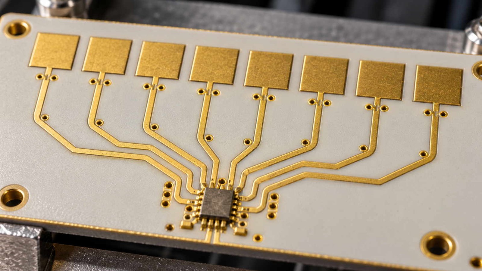
The distinction that matters in a review is between errors that are constant per channel and errors that are dispersive. Length differences are the first kind. Laminate Dk shifts are the second, because they change the guided wavelength and therefore the phase slope. The two require different defences: length matching at layout, and batch control at procurement. The propagation and impedance baselines are set out in our Dk and Df performance and controlled impedance guides.
4. The Link Budget Meets the Loss Budget
At 60 GHz the atmosphere helps and hurts at the same time. The oxygen absorption line around 60 GHz is what makes the band attractive for dense reuse — the signal dies quickly, so it does not travel far enough to interfere — and it is also what limits the link. Over a kilometre the two terms are comparable.
| Budget item | Value | Note |
|---|---|---|
| Free-space path loss, 1 km at 60 GHz | 128.0 dB | 20·log10(4πd/λ), isotropic reference |
| Oxygen absorption, 1 km | ~15 dB | The 60 GHz line is the reason for the band, and the cost |
| Total channel, 1 km | 143.0 dB | Before either antenna gain |
| Feed loss, 1 dB | range −12.2% | Every dB of board loss is bought back in range |
| Feed loss, 3 dB | range −36.6% | Typical spread between a good and a mediocre feed network |
Range sensitivity is 10^(1/20) − 1 per dB at the free-space exponent. It is the clearest argument for treating the feed as a loss-critical structure rather than a connection.
The board's contribution is the part that sits before any of this arithmetic is applied. One dB in the feed is one dB off the top of the link, and at the free-space exponent that is 36.6% of range. On a kilometre-scale link, three decibels of avoidable board loss is a third of the range — which is why the difference between a laminate chosen for loss and one chosen for convenience shows up as a product specification rather than as a cost line.
Loss has two sources on the board, and they respond to different decisions. Dielectric loss follows Df and frequency; conductor loss follows surface roughness and the width the impedance forces on you. The second term is often the larger one at 60 GHz, because a 50 Ω line on 0.127 mm laminate is 0.32 mm wide and carries its current in a skin a fraction of a micron deep — so foil roughness becomes a direct multiplier on insertion loss. The material side of that argument is in our high-frequency PCB materials section and the surface-finish considerations in the RF surface finish guide.
5. Eight Channels in One Enclosure
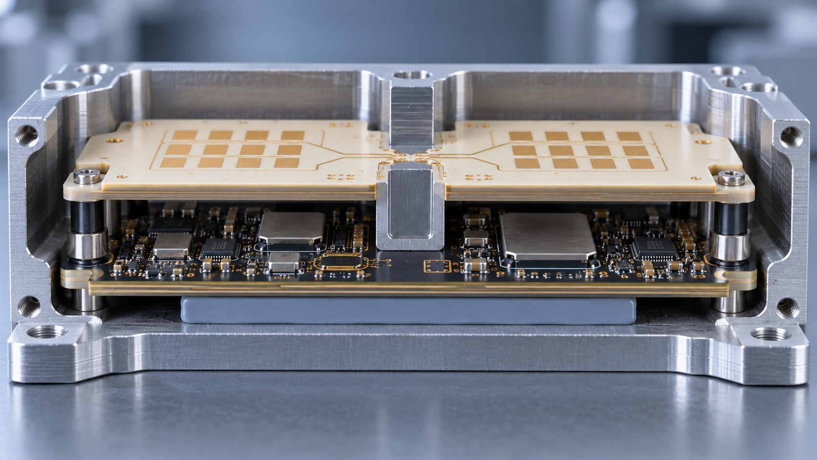
Eight channels at λ0/2 occupy 19.99 mm of aperture, and the module around them has to carry an antenna, an RF section, a control and interface section, and a thermal path — usually in a housing small enough to mount on a pole or a drone. That is a mechanical constraint that arrives before any electrical one.
Three consequences follow. First, the antenna is inside the enclosure's near field, so a metal lid or a radome standoff placed too close shifts the array's impedance and its pattern together — which is why the lid has to be part of the electromagnetic design, not a packaging afterthought. Second, the control and interface section is digital, and it has to be separated from the eight RF channels without cutting the ground plane that those channels need; the partition design is the same problem treated in mixed-signal and high-speed RF board design. Third, the thermal path goes through the same laminate, and on a 0.127 mm low-loss material that path is poor — the module lid or a thermal pad does most of the work.
Assembly is a decision, not a detail. A connectorised module puts eight launches on the board, each of which is a discontinuity that has to be characterised; a board-to-board or antenna-in-package approach moves that discontinuity outside the board. Both are defensible, and the choice changes what the first-article package must contain. The assembly routes are covered in our antenna module PCB assembly and RF PCB assembly guides.
6. What a First Article Must Prove
There is an order in which measurements make sense, and it is not the order in which they are usually requested.
Per-channel electrical length comes first, because it is the only property that later measurements cannot separate from the antenna. If the eight channels arrive with a phase spread, every pattern measurement afterwards contains that spread as an unknown. Impedance comes second, per panel, because a return loss problem at the band edges shows up as gain that disappears where the design intended it to be flat. Isolation — cross-polarisation and beam-to-beam — comes third, because it is measured through the same setup as the pattern and is meaningless without a known phase reference.
What is often skipped is the coupon that carries the real launch geometry. A coupon that measures 50 Ω on a straight line proves the stackup; it does not prove that the eight launches into the antenna are identical. If the coupon is to mean anything, it has to carry the structure being qualified — the same argument we make about reference planes in the mmWave VNA testing guide and about launch geometry in the RF connector launch guide.
7. The 57–70 GHz Module RFQ Checklist
Related reading
- 77 GHz radar SoC PCB design for 4T4R — virtual-array pitch, the phase budget in degrees per millimetre, and Dk batch tolerance
- 1 mm switch-connector RF test point DFM — pad geometry, ground-return inductance and probe keep-out at 15 GHz
- 5G mmWave PCB overview — the wider picture from 24 GHz to 40 GHz
- 60 GHz in-cabin radar PCB — the sensing side of the same 57–71 GHz band
Eight lines, each of which maps to a number computed on this page.
| # | Item to specify | Why it decides the outcome |
|---|---|---|
| 1 | Band edges and centre frequency | Sets the pitch compromise and the loss budget |
| 2 | Number of channels and polarisation scheme | Fixes the aperture and the feed topology |
| 3 | Beam count and required isolation between beams | A layout property, not a device property |
| 4 | Laminate, thickness and copper weight | Guided wavelength, loss and thermal path together |
| 5 | Phase and amplitude match, in degrees and dB | The two numbers that cannot be fixed after lamination |
| 6 | Enclosure interface: radome, lid, thermal pad | The lid is inside the antenna's near field |
| 7 | Assembly: connectorised or board-to-board | Decides whether launch structures are on this board at all |
| 8 | Required evidence package | Coupons, per-channel length, isolation measurement |
Eight lines. The first three decide the design; the last five decide whether it repeats in production.
The pattern: a wideband dual-beam module is specified by band edges and matching, and proved by per-channel records. The silicon decides how fast the link runs; the laminate and the length matching decide whether both beams point where the schedule says they do.
60 GHz Communication Module PCB — Frequently Asked Questions
Dual-beam isolation, 0.1 mm phase arithmetic, element pitch across 57–70 GHz, loss-to-range conversion and what to measure first on a first article.
Is a 60 GHz communication module the same board as a 60 GHz radar?
No, and the difference is in what the layout has to preserve. A radar board is judged on range resolution and detection, which are set by bandwidth and by the chirp chain. A communication module is judged on link margin, which is set by absolute loss and by how well eight channels hold their relative phase and amplitude. The same laminate and similar stackups appear in both, but the tolerance that dominates is different — chirp linearity there, channel matching here. Our 60 GHz in-cabin radar PCB guide covers the sensing case.
Why does 0.1 mm of trace matter at 60 GHz?
Because the guided wavelength on 0.127 mm laminate is 3.208 mm, so the phase sensitivity is 112.2° per millimetre. A 5-bit phase shifter resolves 11.25°, which is 0.100 mm of line. A tenth of a millimetre is therefore a full resolution step: the board can move the beam by one increment on its own, before any calibration is applied.
Does the wide 57–70 GHz band force a narrower element pitch?
It forces a decision. λ0/2 is 2.63 mm at 57 GHz and 2.14 mm at 70 GHz — an 18.6% spread. An array fixed at the 60 GHz value will show grating-lobe onset at the top of the band when scanned hard, and slightly wider spacing than ideal at the bottom. The usual compromise is to design at the highest frequency that must scan, and accept marginally closer spacing at the low end, where the loss from mutual coupling is smaller.
How much does the feed network cost in range?
One dB of feed loss costs about 12.2% of link range at the free-space exponent, so 3 dB costs 36.6%. On a 1 km link that is the difference between closing and not closing. This is why the feed is specified as a loss budget line item rather than as a routing detail.
Can the module be assembled on a hybrid stack with a cheaper digital section?
Yes, and it usually should be, because the control, power and interface section does not need the loss performance of the antenna region. The constraint is the transition between the two material regions: it has to be placed where a via or a controlled launch can bridge them without an uncontrolled stub. The trade-offs are worked through in our FR4 and high-frequency hybrid and multilayer high-frequency guides.
What is the first thing to measure on a first article?
Per-channel electrical length, before any pattern measurement. If the eight channels do not match in phase, every later measurement is confounded by a pointing error that looks like an antenna problem. Phase match is the one board property that a pattern measurement cannot separate from the antenna design.
Building a 57–70 GHz module with two beams?
Send the band edges, the channel count, the polarisation scheme and your phase and amplitude match targets. We will convert them into length and Dk allowances, choose laminate and copper weight against the loss budget, place the hybrid transition, and ship the first-article package — per-channel length report, insertion loss coupon and isolation measurement — with the boards to IPC Class 3.
Contact Us → WhatsApp: +86 137 6047 3650Request a PCB Quote
Upload your Gerber ZIP file and project requirements. Our engineering team will review your PCB material, stackup, impedance needs, surface finish, and production quantity before quoting.
Please prepare:
- Gerber files in ZIP format
- PCB material or stackup requirements
- Controlled impedance notes if available
- Prototype or batch production quantity