
77 GHz Radar SoC PCB Design: Four Transmitters, Four Receivers and the Tolerances They Expose
77 GHz radar SoC PCB design for 4T4R automotive radar: virtual-array pitch, 144 degrees per millimetre, Dk batch limits, thermal vias and the evidence package.
Home » 4T4R MIMO Radar » 77 GHz Radar SoC PCB Design: Four Transmitters, Four Receivers and the Tolerances They Expose
Table of Contents
Integrating four transmitters, four receivers, the chirp generator, the DSP and the microcontroller into one 22 nm FD-SOI package looks like a simplification. On the board it is a transfer: eight RF ports that used to be spread across several devices now converge in one footprint, and every one of them carries a phase relationship that the system depends on. The package did not remove the analog work. It concentrated it into a few square centimetres of laminate.
The numbers below are what that concentration costs. A quarter-wavelength at 77 GHz is under a millimetre; a tenth of a millimetre of extra trace is 14.4 degrees; a laminate batch that arrives 0.04 higher in Dk moves phase more than the etch tolerance ever will. None of these are exotic — they are ordinary fabrication variables, and they are the reason two radar boards built to the same Gerber file can rank differently in the same test cell.
The general automotive context is set out in our automotive radar PCB and 77 GHz radar PCB guides; the array-level view is in the phased array PCB guide. This page is about the specific arithmetic a 4T4R single-chip front end imposes.
1. What a 4T4R SoC Actually Moves onto the Board
Take the published feature set at face value: 76–81 GHz, four transmit channels, four receive channels, an all-digital chirp PLL, DSP, microcontroller, on-chip memory and automotive network interfaces, in 22 nm FD-SOI, with two variants that are pin compatible and differ in on-chip compute. That is a complete radar front end in one package.
| Function | Inside the SX601/SX600 package | What stays on the PCB |
|---|---|---|
| Chirp generation | All-digital chirp PLL, 76–81 GHz | Nothing — but the reference clock must arrive clean |
| Transmit path | 4 transmitters, on-chip power amplifiers | 4 feed lines to 4 antenna ports, phase-matched |
| Receive path | 4 receivers, on-chip LNAs and mixers | 4 feed lines, plus the ground return under each |
| Signal processing | DSP, microcontroller, on-chip memory | Supply decoupling, network interfaces, EMC filter |
| Antenna | Not included — external | Patch array or waveguide transition, on the board |
| Thermal path | Not included — the package is the source | Vias, copper spread, module lid interface |
Package content as published by Bosch for the SX60x family; the right-hand column is the board's remaining scope.
Read the right-hand column again. What remains is not glue logic — it is every structure whose behaviour depends on geometry: eight feed lines that must hold a phase relationship, a ground reference that has to be continuous under all of them, an antenna that is now the largest single contributor to insertion loss, and a thermal path that has to move several watts through a laminate with a thermal conductivity two orders of magnitude below copper.
The integration changed the failure modes too. With discrete front ends, a channel that drifted could be traced to a component. Now every channel shares one die, one reference clock and one thermal environment, so a channel-to-channel error is almost always a board error — and the board is the only place it can be fixed.
2. The Virtual Array Is a PCB Dimension
Four transmitters and four receivers do not give eight independent measurements. Time-multiplexing the transmitters gives eight virtual elements, and the array they form exists only if the physical spacing is right. With receivers at λ0/2, the transmitters must be spaced four times that — the receiver count times the element pitch — so the eight virtual channels land contiguously instead of overlapping.
| Frequency | λ0 in air | λ0/2 | Tx pitch for a contiguous virtual array | Aperture (7 × λ0/2) | Angular resolution |
|---|---|---|---|---|---|
| 76.5 GHz | 3.919 mm | 1.959 mm | 7.84 mm | 13.72 mm | 14.3° |
| 77.0 GHz | 3.893 mm | 1.947 mm | 7.79 mm | 13.63 mm | 14.3° |
| 79.0 GHz | 3.795 mm | 1.897 mm | 7.59 mm | 13.28 mm | 14.3° |
| 81.0 GHz | 3.701 mm | 1.851 mm | 7.40 mm | 12.95 mm | 14.3° |
Angular resolution is 2/N with N = 8 virtual channels (4 Tx × 4 Rx), independent of frequency; the spacing that produces it is not.
At 77 GHz that is 7.79 mm. It is a mechanical dimension on a PCB, subject to the same etch and registration tolerances as any other feature, and it produces an aperture of 13.63 mm supporting roughly 14° of angular resolution. Four receivers alone would give 28.6° — half the resolution — so the transmitter positions are doing real work, and their tolerance is not negotiable in the way an ordinary routing tolerance is.
There is a second-order effect that catches hybrid designs. The pitch is defined in air, because the wave leaving the patch is in air, but the feed network that carries the signal to each element is in laminate. The two media have different wavelengths — 3.893 mm in air against 2.500 mm of guided wavelength — so a feed network that is geometrically symmetric can still be electrically asymmetric if the element launch lengths differ. The array geometry and the feed geometry have to be checked in the same coordinate system. The same discipline appears in X/Ku-band AESA radar boards, where the pitch is larger but the arithmetic is identical.
3. Phase Error in Degrees per Millimetre
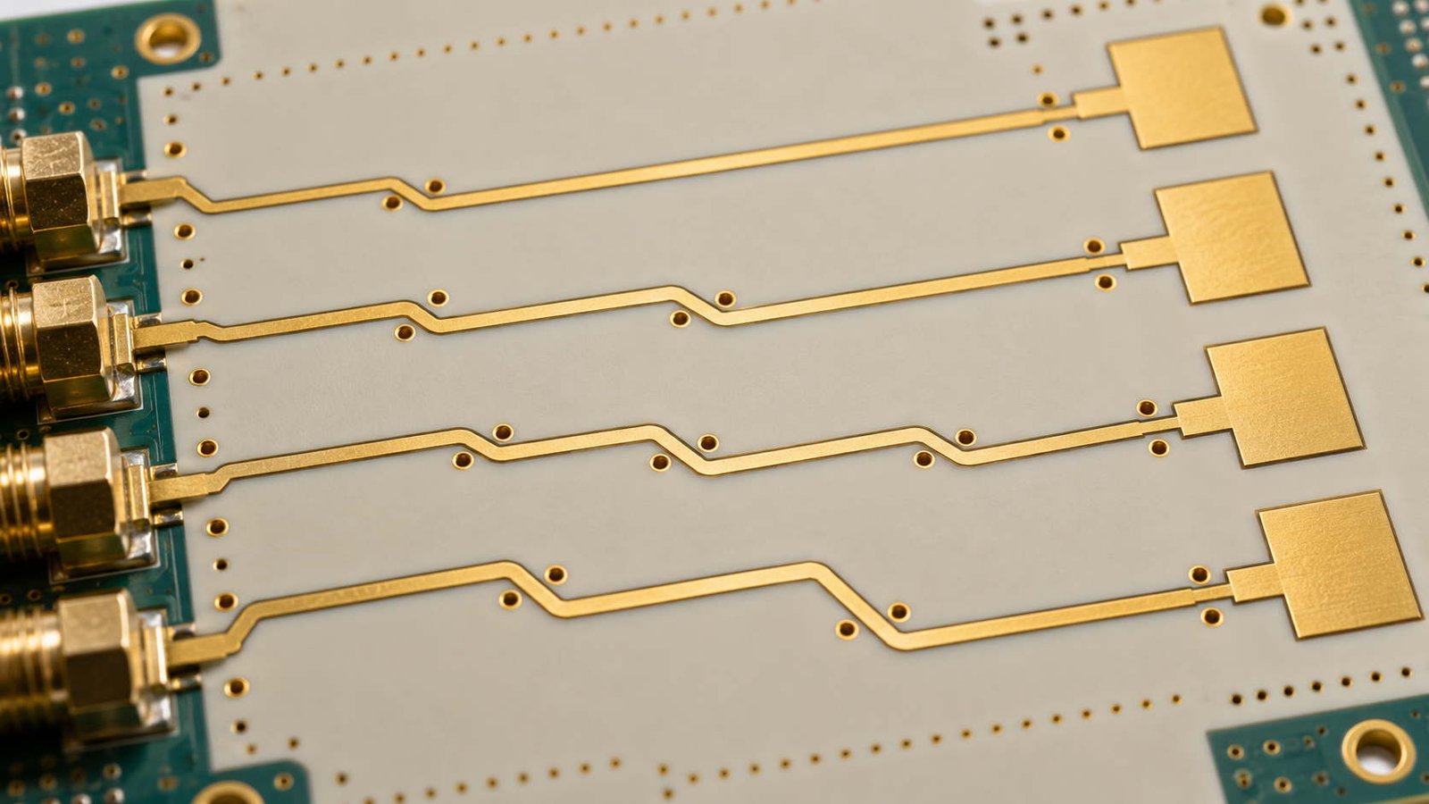
On 0.127 mm laminate with Dk 3.00, a 50 Ω microstrip is 0.321 mm wide — narrow enough that the width tolerance is a few percent of the width itself. The effective permittivity lands at 2.426, the guided wavelength at 77 GHz is 2.500 mm, and the phase sensitivity is therefore 144.0° per millimetre.
| Error source | Physical magnitude | Phase at 77 GHz over 20 mm | Share of a 5° budget |
|---|---|---|---|
| Etch / length difference | 0.1 mm | 28.80° | 288% |
| Etch / length difference | 0.02 mm | 5.76° | 58% |
| Laminate Dk, batch to batch | ΔDk = 0.04 | 16.79° | 336% |
| Laminate thickness | +10% | Z0 → 53.14 Ω | affects return loss, not phase |
| Line width | −0.02 mm | Z0 → 52.10 Ω | affects return loss, not phase |
Phase sensitivity 144.01°/mm on 0.127 mm laminate; a 5° channel-to-channel budget corresponds to 34.7 µm of electrical length. The two rows that exceed the budget cannot be etched away — they are bought.
This is the table that reframes a layout review. A 5° channel-to-channel budget is 34.7 µm of electrical length — thinner than a human hair, and inside the normal etch tolerance band of a production panel. Length matching gets you to the right order of magnitude and no further. The remaining error has to come out of the laminate: a Dk tolerance of ±0.04 moves the phase by 16.79° over 20 mm, which is more than three times that 5° budget.
The practical response is not to demand tighter etch — it is to lock the laminate batch and to prove it. The method, including the impedance and propagation baselines, is set out in the Dk and Df performance guide and the controlled impedance guide; what matters here is that the certificate travels with the lot, not with the order.
4. What the Laminate Choice Actually Buys
At 76–81 GHz the loss budget is dominated by two terms: dielectric loss, which scales with frequency and with Df, and conductor loss, which depends on surface roughness and on how wide the line has to be. The second term is a function of Dk, because a higher Dk means a shorter guided wavelength and a narrower 50 Ω line for the same thickness — more resistance per unit length, but also a smaller radiating patch, which some array designs want.
| Laminate | Dk (10 GHz) | Dk tolerance | Df (10 GHz) | Thermal conductivity | Selection driver |
|---|---|---|---|---|---|
| RO3003 | 3.00 | ±0.04 | 0.0010 | 0.50 W/m·K | Lowest loss at 77 GHz; PTFE-class dimensional behaviour |
| RO4350B | 3.48 | ±0.05 | 0.0037 | 0.69 W/m·K | Higher Dk suits shorter resonant patches; better thermal path |
| RO4835 | 3.48 | ±0.05 | 0.0037 | 0.69 W/m·K | Oxidation-resistant foil for long-life automotive exposure |
Values from the manufacturers' published data sheets at 10 GHz; the selection axis is loss versus thermal conductivity and mechanical stability, not one part standing in for another.
Three axes are being traded here, and it is worth naming them separately. Loss decides how much of the transmit power reaches the antenna and how much receiver sensitivity survives the feed network. Thermal conductivity decides whether heat leaves through the board at all. Dimensional stability decides whether the array pitch survives reflow and thermal cycling. A laminate that is excellent on the first axis can be ordinary on the other two, which is why the choice is a selection among parameters rather than a ranking.
The detail that catches people is that Df matters more than Dk at this frequency. Designers habitually compare Dk values because Dk sets the geometry, but by 77 GHz the dielectric loss tangent is what separates a workable feed network from a marginal one, and the difference between 0.0010 and 0.0037 is a factor of nearly four in that term. The material families and their available thicknesses are collected in our high-frequency PCB materials section.
5. The Transition: Where the Chip Meets the Antenna
Between the package launch and the radiating element there is a transition — a bump or a bond wire, a short length of feed, and either a via to the antenna layer or a direct patch. At 77 GHz, a 1 mm feed is 144° of electrical length, so a transition that adds a quarter of a millimetre of length is a measurable phase step. This is the region where the design is least forgiving and least documented.
| Parameter | Change | Resulting Z0 | Deviation | Verdict against ±5% |
|---|---|---|---|---|
| Nominal | 0.321 mm on 0.127 mm, Dk 3.00 | 50.00 Ω | — | Reference |
| Laminate thickness | +10% | 53.14 Ω | +6.27% | Exceeds ±5% |
| Etched width | −0.02 mm | 52.10 Ω | +4.21% | Inside ±5%, but eats the phase budget |
| Both together | +10% thickness, −0.02 mm width | 55.6 Ω | +11.2% | Fails |
εeff = 2.426, λg = 2.500 mm at 77 GHz for the nominal line. A fabrication lot that drifts on both axes leaves the ±5% impedance window entirely.
A ten percent thickness excursion is not hypothetical — it is what the tolerance on a thin laminate looks like when a lot lands at the edge of the band. On its own it puts Z0 at 53.14 Ω, outside a ±5% window; combined with a modest over-etch it reaches 55 Ω. The reason this matters more at 77 GHz than at 10 GHz is that the return loss penalty is paid where the antenna is already the dominant loss, so the system sees it as reduced range rather than as a reflection.
The launch geometry itself — how the pad is sized, how the ground vias are arranged, how the reference plane transitions — is the subject of the RF connector launch and via design for RF guides, and the waveguide alternative is covered in the PCB to waveguide transition work. What a single-chip radar adds is that there are eight of these transitions in one footprint, all of which must match.
6. Thermal: A Dense Die on a Poor Conductor
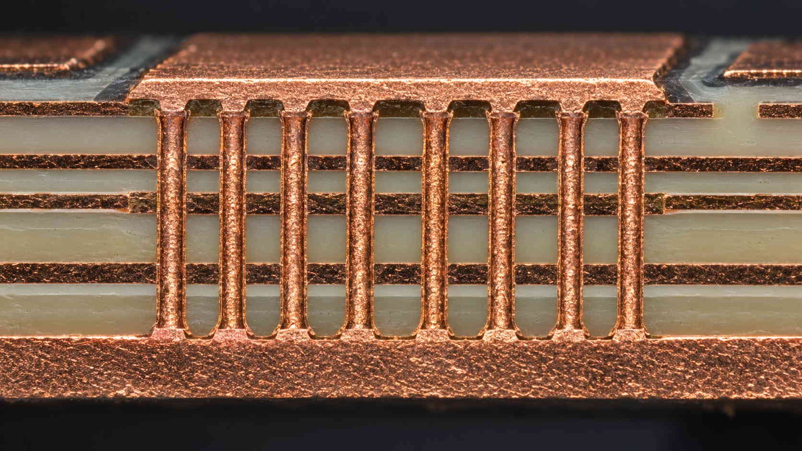
The dielectric under a radar SoC conducts heat at 0.50 W/m·K. Copper conducts at roughly 400. So the vertical path through the laminate is not a path at all — it is a wall, unless it is filled with vias. That is why the via field exists, and it is also why adding vias past a certain count stops helping.
| Thermal path element | Per unit | At 16 vias / 1 cm² | Comment |
|---|---|---|---|
| Plated via, 0.3 mm drill, 0.197 mm long | 6.95 K/W | 0.434 K/W (16 vias) | Copper-filled or plated, either way the barrel does the work |
| Plated via, 25 vias | 6.95 K/W | 0.278 K/W (25 vias) | Diminishing return: beyond this the lid dominates |
| Dielectric, vertical, RO3003 | 2.54 K/W per cm² | — | 0.127 mm of 0.50 W/m·K material is not the bottleneck |
| Same, FR4-class material | 4.23 K/W per cm² | — | For comparison on a hybrid stack only |
Per-watt figures: multiply by dissipated power. The decision that matters is copper spread area and the lid interface, not adding a seventeenth via.
Sixteen vias get the via path to 0.43 K/W; twenty-five get it to 0.28 K/W, a 56% improvement in a term that is already small compared with the lid interface and the spread resistance in the copper. In a practical module the bulk of the heat leaves through the top of the package into a thermal pad or a metal lid, and the vias handle what escapes downward into the board. Sizing the field is therefore a spreading question: how much copper area is available on the far side, and how is it connected to the housing.
Two consequences for the layout. First, the ground plane under the die should be continuous and as large as the RF constraint allows, because it is both the RF reference and the thermal spreader — those two requirements happen to agree. Second, a hybrid stack that puts a thermally better material under the die and a lower-loss material under the antenna trades thermal performance for electrical performance in a way that has to be decided before the stackup is frozen; the trade-offs are worked through in the FR4 and high-frequency hybrid guide and the multilayer high-frequency guide.
7. One Footprint, Two Compute Tiers
Pin compatibility between the two variants is a genuine convenience for a product family — one board, two price points — but it is a constraint on the layout, not a freedom in procurement.
| SX601 | SX600 | |
|---|---|---|
| Process | 22 nm FD-SOI RF-CMOS | 22 nm FD-SOI RF-CMOS |
| Frequency | 76–81 GHz | 76–81 GHz |
| Channels | 4 Tx / 4 Rx | 4 Tx / 4 Rx |
| On-chip compute | Higher — sensor fusion, classification, tracking | Lower — detection and raw processing |
| Package / pinout | Pin compatible | Pin compatible |
| PCB consequence | Thermal and decoupling design set by this part | Same board, reduced BOM |
As published by Bosch for the SX60x family. Pin compatibility is a board-design constraint, not a procurement convenience: one layout must satisfy the hotter of the two.
The rule that follows is simple and frequently broken: design the board for the hotter part. Decoupling, copper area, via count and lid interface must all satisfy the higher-compute variant, because the footprint cannot change when the product line is upgraded. A board designed around the lower tier will pass its own validation and then fail when the same layout is populated with the other part — and by then the qualification is done against the wrong thermal case.
8. The Evidence Package, and the RFQ Checklist
Related reading
- 60 GHz dual-beam communication module PCB — element pitch, beam-to-beam isolation and the 57–70 GHz loss budget
- 1 mm switch-connector RF test point DFM — pad geometry, ground-return inductance and probe keep-out at 15 GHz
- W-band noise figure measurement on PCB — Y-factor arithmetic, source match uncertainty and the finish that decides 75–110 GHz
- 77 GHz radar PCB manufacturing — material, stack-up and via rules for 76–81 GHz hardware
- automotive radar PCB qualification — PPAP evidence, thermal cycling and the audit trail
An automotive radar board is unusual in that most of its critical parameters become invisible as soon as it is assembled. The dielectric thickness, the plating in a via barrel, the final etched width under a patch, the registration of a ground ring — none of them can be measured on the finished module. The evidence package is therefore not documentation; it is the only record that the board is what it was supposed to be.
| Evidence | What it proves | When it is produced |
|---|---|---|
| Dk / Df certificate per laminate lot | A batch change did not move the phase | Every lot, before drilling |
| Impedance coupon, per panel | Z0 within ±5% after etch | Every panel |
| Per-channel electrical length report | Channel-to-channel phase inside budget | First article and on change |
| Cross-section | Plating, dielectric thickness, mask dam | First article |
| Cpk on antenna feature position | Array pitch is a controlled dimension | First article |
| Thermal cycling, −40 to +125 °C | Via and plated-through integrity | Qualification |
| Ion contamination report | Cleanliness for a sealed module | Qualification |
The automotive file is not paperwork added at the end; each line is the only record of a parameter that is invisible once the module is potted.
Each line maps to a number computed earlier on this page. The impedance coupon guards the ±5% window. The per-channel length report guards the phase budget. The Dk certificate guards the batch shift that no amount of etch control can recover. The Cpk on array pitch guards the virtual array itself. Remove any one and a corresponding error becomes undetectable.
| # | Item to specify | Why it decides the outcome |
|---|---|---|
| 1 | SoC part number and compute tier | Fixes the thermal design point for the whole layout |
| 2 | Antenna type: patch array or waveguide transition | Two different stackups, two different tolerances |
| 3 | Required channel-to-channel phase match, in degrees | Converts directly to a length and Dk budget |
| 4 | Laminate family, thickness and copper weight | Sets λg, Z0 and the thermal path at once |
| 5 | Tx and Rx element pitch, with tolerance | The virtual array only exists if the pitch is controlled |
| 6 | Finish and its thickness at 77 GHz | Skin depth at 77 GHz is sub-micron; nickel is not optional |
| 7 | Thermal interface and lid arrangement | Bulk of the heat leaves through the lid, not the vias |
| 8 | Qualification level and the evidence package | IATF 16949 line, PPAP, and the reports listed above |
Eight lines. Every one of them is cheaper to agree before layout than to discover in a first article.
The pattern across all eight lines is the same: a 4T4R radar board is specified mostly in geometry and tolerance, and proven mostly by records. The silicon decides what the radar can do; the laminate and the plating decide whether it does it the same way on the ten-thousandth unit as on the first.
77 GHz Radar SoC PCB — Frequently Asked Questions
Virtual-array pitch, phase budgeting in degrees per millimetre, Dk batch tolerance, finish at 77 GHz and how many thermal vias a radar SoC actually needs.
Why does transmitter pitch matter on the PCB?
Because the virtual array is built from geometry. With four receivers spaced λ0/2 apart, the four transmitters must sit four times that distance apart — 7.79 mm at 77 GHz — so that the eight virtual channels interleave without a gap or an overlap. A pitch error of 0.1 mm is not a gain error; it is a phase error of 14.4° between adjacent virtual elements, which shows up as a sidelobe and an angular bias.
How tight must channel-to-channel length matching be at 77 GHz?
On 0.127 mm laminate the guided wavelength is 2.50 mm, which is 144.0° per millimetre. A 5° budget is therefore 34.7 µm of length. That is inside normal etch tolerance, which is why length matching alone is not sufficient — the laminate Dk tolerance has to be controlled as well, because a Dk shift of 0.04 moves the phase more than 0.1 mm of length does over a 20 mm run.
Does a 4T4R SoC reduce the number of board layers?
Not necessarily. It removes external RF switches and discrete LNAs, which frees area, but it concentrates eight RF ports plus digital, clock and power in one region. In practice the stackup is driven by the need for a continuous ground reference under all eight feeds and a clean return path for the chirp reference clock — not by the component count.
What finish is appropriate for a 77 GHz radar board?
The finish has to survive at the highest frequency on the board and must not introduce a magnetic layer in the current path. At 77 GHz the skin depth in gold is a fraction of a micron, so a thin immersion gold over nickel behaves acceptably; the same stack at low frequency does not, because the current reaches the nickel. Specify the finish by the lowest frequency that actually carries current, not by the headline frequency.
How many thermal vias does a radar SoC actually need?
Fewer than most layouts assume. Each 0.3 mm via through a 0.127 mm laminate is about 7.0 K/W, so sixteen in parallel are 0.43 K/W and twenty-five are 0.28 K/W — the second thirteen vias buy 0.16 K/W. The lid interface and the copper spread area dominate the total. Sizing the via field is a spreading problem, not a counting problem.
Can one board design serve both compute tiers?
Yes, and Bosch makes that practical by keeping the two parts pin compatible. The consequence is that the layout must be designed to the thermal and decoupling worst case of the higher tier, because the footprint cannot change between them. Designing to the lower tier and upgrading later is not an option once the board is cut.
Building a 4T4R radar board at 76–81 GHz?
Send the SoC part number, the antenna type and your channel-to-channel phase budget in degrees. We will convert it into a length and Dk allowance, choose the laminate and copper weight against the thermal path, define the via field and the finish by frequency, and ship the first-article package — impedance coupons, per-channel length report, cross-section and Cpk on the array pitch — with the boards to IPC Class 3.
Contact Us → WhatsApp: +86 137 6047 3650Request a PCB Quote
Upload your Gerber ZIP file and project requirements. Our engineering team will review your PCB material, stackup, impedance needs, surface finish, and production quantity before quoting.
Please prepare:
- Gerber files in ZIP format
- PCB material or stackup requirements
- Controlled impedance notes if available
- Prototype or batch production quantity