
Radar PCB Manufacturer: S/C-Band to 79 GHz, Materials In Stock and TDR-Verified Lots
Radar PCB manufacturing from a direct factory: band-by-band requirements from 24 GHz SRR to 77/79 GHz automotive front radar and defense SAR, material selection, via fencing, tolerance control and the QC evidence to ask for.
Home » 77 GHz Radar PCB » Radar PCB Manufacturer: S/C-Band to 79 GHz, Materials In Stock and TDR-Verified Lots
Table of Contents
Radar is the application that stresses every discipline a high-frequency PCB factory has at once: a dielectric constant held to a few hundredths, ground structures stitched at fractions of a millimetre, hybrid stackups that carry RF and digital on one board, and an impedance figure that has to be measured, not assumed. A radar PCB manufacturer is therefore judged on the lot, not on the sample.
This page is the overview of how we build radar boards from S/C-band weather radar to 79 GHz automotive front ends: what changes with frequency band, which laminates are on the shelf and where each one fits, how impedance is verified on every lot, and the structuring work — via fence, back drilling, hybrid lamination — that the band forces. Band-level detail lives on the dedicated pages: 77 GHz radar PCB manufacturing, the X/Ku-band AESA radar PCB guide, and the automotive radar PCB review.
1. What Radar PCB Manufacturing Covers
Radar boards span an unusual range of build types for one product family. At the low end, a weather or surveillance radar in S or C band is a large multilayer whose difficulty is layer count, planarity and cost. In X and Ku band, the board becomes a controlled-impedance PTFE structure, often with the digital processing sharing the same panel. At 24, 60, 77 and 79 GHz, the board is an antenna in its own right: the radiating elements, the feed network and the ground structures are the board, and every fabrication tolerance lands directly on the beam.
What stays constant across that range is the discipline. The material has to be what the drawing says, verified by certificate rather than by reputation. The impedance has to be measured on the lot. The ground return has to be stitched deliberately. And the factory has to hold all of it on a production schedule, not on a golden sample.
That is the sense in which “radar PCB manufacturer” is a real distinction rather than a keyword. The band pages on this site — Ka-band, 77 GHz, AESA, automotive — each describe the same factory from a different band’s point of view; this page describes the factory itself.
2. What Changes With Frequency Band
Wavelength is the master variable. Everything that is a comfortable number at 3 GHz becomes a tight one at 77 GHz, and the tightness is not linear — the ground structures and etch tolerances that were rounding errors at X band are the dominant design constraint at 77 GHz:
| Radar band | Free-space λ₀ | What the PCB build has to hold |
|---|---|---|
| S/C band — weather and surveillance radar (2–8 GHz) | 150 – 37.5 mm | Large-format multilayers; the challenge is layer count and planarity, not geometry |
| X band — military and marine radar (8–12 GHz) | 37.5 – 25 mm | Low-loss PTFE builds, controlled impedance feed networks, thermal management on transmit modules |
| Ku band — satellite and mapping radar (12–18 GHz) | 25 – 16.7 mm | Tighter etch control; hybrid stackups carrying digital processing alongside the RF front end |
| 24 GHz — legacy automotive short-range radar | 12.5 mm | Cost-controlled antenna boards at automotive quality-system discipline |
| 60 GHz — short-range imaging and sensing | 5.0 mm | Ground-via pitch under 0.4 mm; every extra mil of trace tolerance becomes phase error |
| 77 / 79 GHz — automotive long-range radar | 3.9 – 3.8 mm | The hardest common case: λg/10 ground stitching near 0.2 mm, back drilling, and Dk tolerance that keeps element resonance on frequency across the lot |
λ₀ = 300 mm/GHz ÷ f (GHz). The band rows name the build consequence, not the application marketing — each of these is treated in depth on its own band page linked from the body text.
The 77/79 GHz row is worth dwelling on because it compresses every discipline at once. At 77 GHz the free-space wavelength is 3.9 mm, and on a Dk 3.48 laminate the guided wavelength is 2.1 mm — so a quarter-wave section is about half a millimetre, and the λg/10 ground stitching rule lands near 0.21 mm pitch. Those two numbers alone decide the drill map, the etch tolerance budget and the price of the board. The full design treatment is in the 77 GHz radar PCB design guide, and the Ka-band context around it in the Ka-band PCB review.
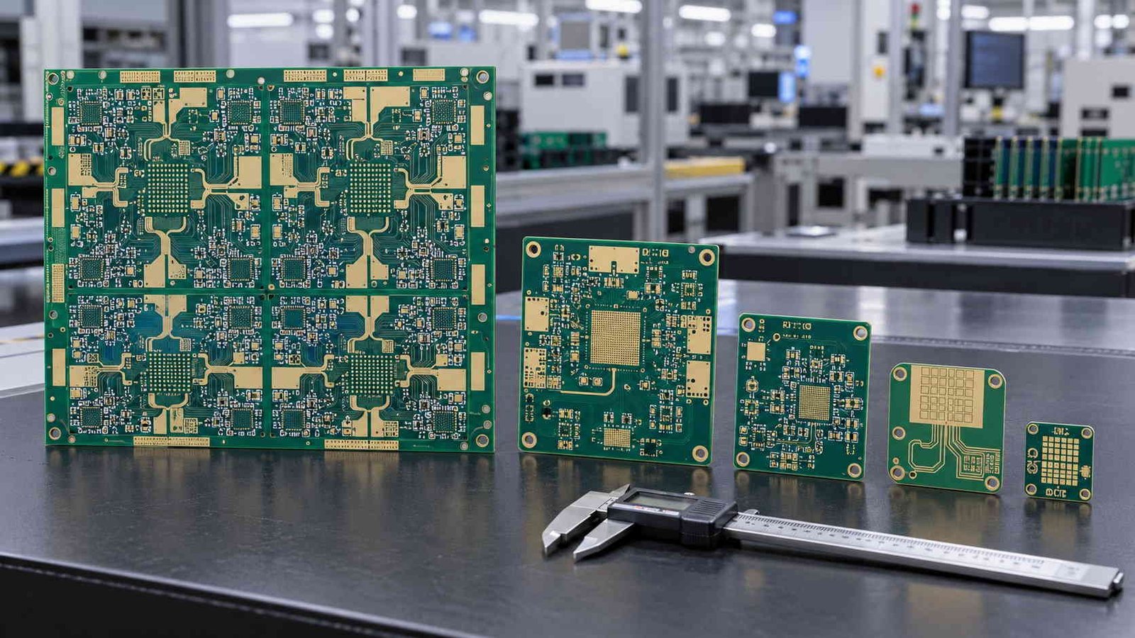
3. Materials In Stock and Where Each One Fits
Material availability is the first schedule question on any radar programme: a factory that buys laminate per order adds weeks before the first panel is imaged. The radar-relevant materials on our shelf, and where each one is normally used:
| Laminate | Where it sits in radar work | Published figures that matter |
|---|---|---|
| Rogers RO3003 | 77 GHz and Ka-band antenna boards; the automotive long-range workhorse | Process Dk 3.00 ± 0.04, Df 0.0010 @ 10 GHz, stable over temperature |
| Rogers RO4350B / RO4003C | 24 GHz and 77 GHz front ends; processed like epoxy/glass | Process Dk 3.48 ± 0.05 / 3.38 ± 0.05, low-loss thermoset route |
| Rogers RT/duroid 5880 | Wideband and EW-grade radar where the lowest loss wins | Dk 2.20, Df 0.0009 @ 10 GHz, PTFE glass microfibre |
| F4B grades | Cost-sensitive antenna and feed layers at Dk 2.2 – 6.15 | Domestic PTFE glass laminates spanning a wide Dk range |
| Taconic laminates (TLY-5, RF-35…) | Antenna and feed layers where availability and price meet | Low-loss PTFE glass grades across Dk 2.2 – 3.5 |
Materials on the shelf, not a sourcing promise made per enquiry. The parameter rows are the published headline figures quoted on each grade page; lot-level values come from the material certificate. Grades are listed side by side as facts — the choice is made on band, loss budget and cost target.
Each grade has its own parameter page on this site — Rogers RO3003 PCB and Rogers RO4350B PCB carry the full data-sheet tables. The grades above are listed as parameter facts; selecting between them is a design decision made on the loss budget, the Dk tolerance the elements need and the cost target of the programme.
4. Impedance Control and Coupon Verification
On a radar board, impedance is a functional parameter: a feed network cut to the wrong impedance is an amplitude and phase error at the elements, which is a pointing error at the beam. So the impedance figure has to be a measured property of each production lot. The capability behind that:
| Item | Capability |
|---|---|
| Materials in stock | Rogers RO4350B, RO4003C, RO3003, RT5880; PTFE laminates; F4B; Taconic laminates |
| Prototype lead time | 7–10 days, no MOQ — material is already on the shelf, so no waiting for laminate procurement |
| PTFE processing | In-house plasma activation before electroless copper, avoiding the smear-related via failures common when this step is outsourced |
| Impedance control | TDR verification to ±5% on every production lot, with impedance reports shipped with the boards |
| Mixed stackups | FR4 + Rogers and FR4 + PTFE hybrid lamination, including bondply selection and lamination cycle control |
| Quality systems | IATF 16949 certified manufacturing for automotive radar programs |
The same capability table published on our RF PCB manufacturer page — radar boards are built on the same line, under the same quality system, and with the same impedance discipline.
The table is deliberately identical to the one on our radar system high frequency PCB application page and our general RF manufacturing page — radar boards run on the same line, under the same quality system, with the same TDR discipline. What radar adds is the verification plan around it, which is set out in the QC section below. The impedance method itself — design Dk versus process Dk, and why the solver value matters — is treated in the controlled impedance RF PCB note.
5. Ground Structures: Via Fence Pitch and Back Drilling
Two structuring operations dominate radar board manufacturing, and both scale with wavelength:
| Frequency | λg on Dk 3.48 laminate | Via fence pitch, λg / 10 |
|---|---|---|
| 10 GHz | 16.1 mm | 1.61 mm |
| 24 GHz | 6.7 mm | 0.67 mm |
| 28 GHz | 5.7 mm | 0.57 mm |
| 38 GHz | 4.2 mm | 0.42 mm |
| 60 GHz | 2.7 mm | 0.27 mm |
| 77 GHz | 2.1 mm | 0.21 mm |
Computed as λg = λ₀/√Dk with the process Dk 3.48 of RO4350B, then divided by ten. Pitch is the single most under-quoted number on a radar board enquiry — it decides drill density, and drill density decides both price and whether the layout is manufacturable at all.
Via fence pitch is the number most often left out of an enquiry, and it is the one that changes the quote the most: the difference between 1.61 mm and 0.21 mm pitch is the difference between two entirely different drill programmes. The stitching rules — pitch, fence placement, interaction with radiating elements — are set out in our via fence PCB guide.
Back drilling removes the stub of a plated through-hole that remains after layer transfer, and on radar boards it is what keeps the stub from acting as a resonant radiator inside the RF structure. Stub length, depth control and the tolerance stack it needs are covered in the back drill PCB guide, and the drilling capability behind both operations in our high frequency PCB drilling capabilities note.
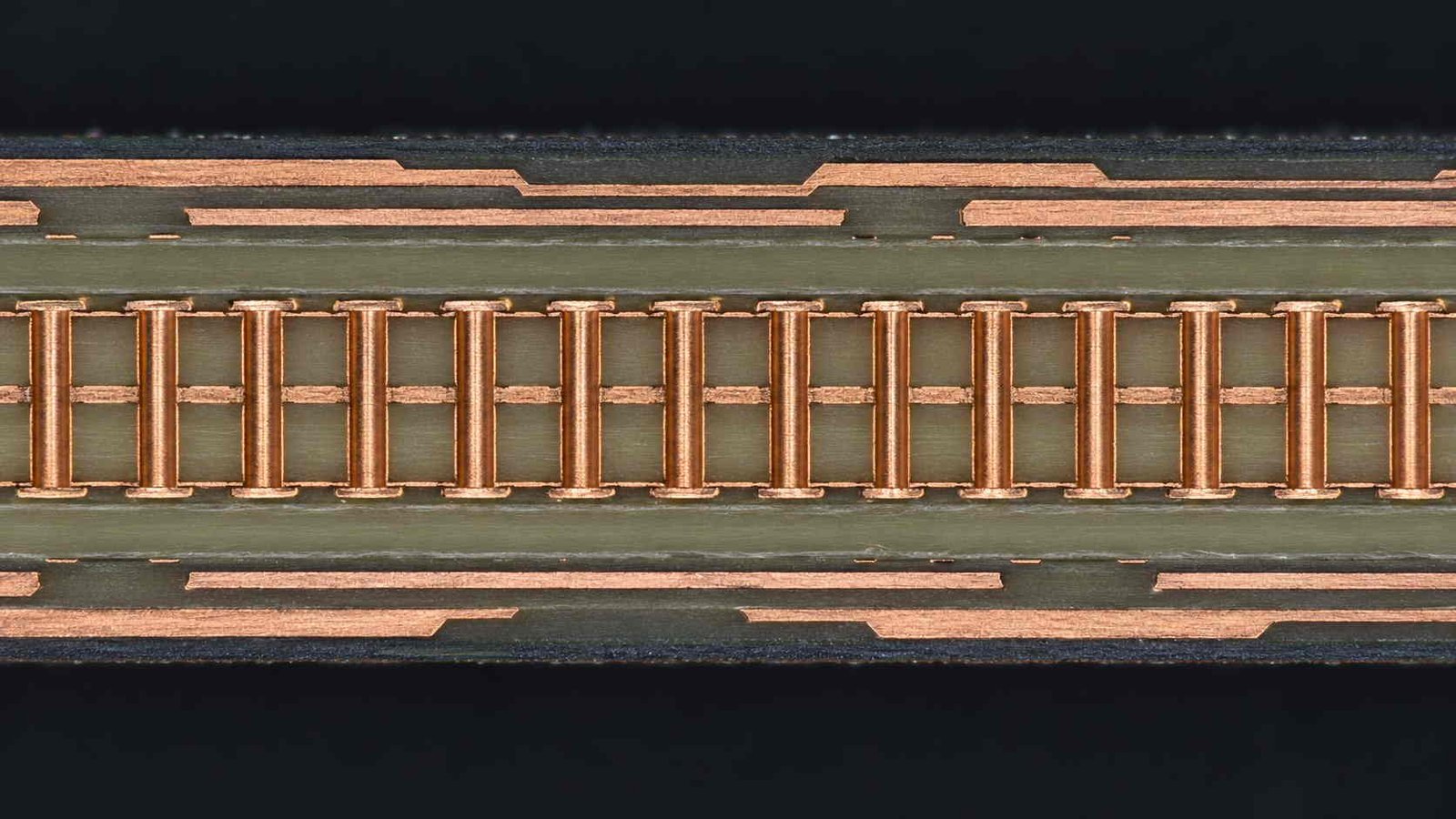
6. Hybrid Stackups: RF and Digital on One Board
Most radar programmes above prototype scale end up asking the same question: does the RF front end stay on its own board, or does it share a panel with the digital processing? Sharing is cheaper to assemble and removes interconnects between the front end and the processor — but it means one lamination cycle has to serve two material systems with different expansion behaviour and different press windows.
That is the hybrid stackup problem: FR-4 layers for power and digital, a low-loss laminate for the RF layers, bonded in a single press cycle with the bondply chosen for the material pair. It is routine on our line — the capability table names it explicitly — but it is also where the lamination cycle control matters, because the PTFE-family layers and the epoxy layers do not forgive the same process window equally.
The design-side view — when a hybrid pays off, the stackup options and the cost trade against a full high-frequency build — is worked through in our FR4 Rogers hybrid PCB review. The manufacturing-side requirement is simpler to state: the stackup, the bondply and the cycle are agreed before the first panel, and the RF reference planes are planned against the digital ground, not discovered after it.
7. QC and Test Plan for Radar Boards
The test plan is where a radar build is won or lost, because the failure modes that matter — impedance drift, stub resonance, via smear, warp on a large antenna panel — are all invisible on a finished board. The plan we propose:
| Checkpoint | What is verified | On what |
|---|---|---|
| Impedance | TDR against the agreed design Dk, ±5% window | Coupon built on the production panel edge, every lot |
| Insertion loss | VNA sweep of the trace-loss coupon against the loss budget | mmWave lots; report shipped with the boards |
| Via integrity | X-ray on buried and blind structures; cross-section on first articles | First article and per-lot sampling |
| Drill quality | Hole-wall smear check on PTFE builds (plasma desmear verified) | First article, and any new material-thickness combination |
| Flatness and warp | Panel warp against the assembly requirement | Large antenna panels before packing |
| Traceability | Material certificate matched to the build lot | Every production lot |
The test plan we propose on a radar RFQ. The first three rows are the ones radar customers audit; the material certificate row is what makes the Dk tolerance in the datasheet mean something for the lot actually built.
At millimetre-wave bands the VNA row is the one that carries the most weight, and the data to demand from any supplier — VNA-verified loss figures, not simulated ones — is set out in our mmWave PCB VNA testing guide.
8. What to Send With a Radar PCB RFQ
A radar RFQ quotes fast when the tolerance stack is visible up front. The list below is what makes that possible:
| Send with the RFQ | Why we ask for it |
|---|---|
| Frequency band and the data rate / range target behind it | The band sets the material class, the via fence pitch and the tolerance stack before anything else |
| Stackup with layer functions marked (RF, digital, power) | Radar boards are usually hybrids; the RF layers get a different material and a different tolerance than the digital ones |
| Impedance targets and the Dk figure they were computed with | Prevents the coupon-versus-simulation argument; we verify against the figure agreed in writing |
| Via fence pitch as drawn, or the drawing itself | We check manufacturability of the pitch before quoting, not after the drill file arrives |
| Back-drill depths, if the build has them | Back drilling is a stackup-height calculation; it needs the full stackup, not just the RF layers |
| PIM requirement, if the antenna is transmit-receive | Foil type and surface finish are chosen for PIM, and the QC plan gains a PIM row |
| Quantity ramp — prototypes to series | Material stocking and lot TDR planning follow the ramp, and prototypes to series should not change material mid-way |
The list that turns a radar RFQ into a quotable build. Everything on it is answerable from the design files you already have.
Send the package through the contact page or WhatsApp, and we will come back with the material confirmation, the manufacturability check on the via fence and back-drill callouts, and a quote with the coupon test plan attached.
Radar PCB Manufacturer — Frequently Asked Questions
What separates a radar-capable factory from a generic one, material choices by band, impedance verification, and RF-digital integration.
What does a radar PCB manufacturer need to hold that a generic PCB factory does not?
Three things. First, material: the radar bands live on low-loss PTFE and ceramic-filled laminates, and the factory has to stock them rather than buy them per order. Second, process: PTFE needs its own plasma desmear and drilling parameters, and a mixed FR4-Rogers stackup needs lamination cycle control so the two material systems survive one press cycle together. Third, verification: impedance on a radar board is a functional requirement, so the lot needs coupon TDR data — at our factory to ±5% on every production lot — rather than a one-off sign-off sample.
Which material is used for a 77 GHz automotive radar board?
The common choice is a ceramic-filled hydrocarbon laminate — Rogers RO3003 (process Dk 3.00 ± 0.04) or RO4350B (3.48 ± 0.05) — because at 77 GHz the dielectric loss and the Dk tolerance both land directly on antenna performance, and RO4350B in particular processes on standard epoxy/glass lines. The 77 GHz case is also where the mechanical structure bites: ground stitching at roughly 0.21 mm pitch on λg/10, back drilling of through-hole stubs, and etch tolerance that is a noticeable fraction of the element dimensions. The band is treated in detail on our 77 GHz radar PCB pages.
How is impedance verified on a radar PCB lot?
On a coupon built on the production panel edge, measured by TDR against the design Dk agreed in writing at quotation. The window we hold is ±5%, and the impedance report ships with the boards. At millimetre-wave bands the coupon carries an insertion-loss structure as well, so the VNA sweep verifies the loss budget, not just the impedance. That is what makes the tolerance stack measurable on the lot actually built instead of on a golden sample that never went through the production press.
Can radar RF and digital processing share one board?
Yes, and it is the normal case at Ku band and below: a hybrid stackup with the RF layers on low-loss laminate and the digital and power layers on FR-4, laminated as one board. The design work is in the stackup — bondply selection, lamination cycle, and where the RF reference planes sit relative to the digital ground. Done deliberately, the hybrid build removes a connector and a cable; done casually, it couples the digital noise into the radar front end. Our FR4 Rogers hybrid PCB review covers the stackup options and the cost trade-off.
Quoting a radar board?
Send the band, the stackup and the impedance targets. We will confirm the material against what is on the shelf, check the via fence pitch and back-drill depths for manufacturability before quoting, and build with coupon TDR data on the lot we actually ship.
Contact Us → WhatsApp: +86 137 6047 3650Request a PCB Quote
Upload your Gerber ZIP file and project requirements. Our engineering team will review your PCB material, stackup, impedance needs, surface finish, and production quantity before quoting.
Please prepare:
- Gerber files in ZIP format
- PCB material or stackup requirements
- Controlled impedance notes if available
- Prototype or batch production quantity