
5G PA Board Design for DTX and Envelope Tracking: The Charge Account Behind the Savings
5G PA board power integrity for DTX and envelope tracking: the charge account behind 36% energy savings, decoupling bands and ground-return design.
Home » 5G Base Station PCB » 5G PA Board Design for DTX and Envelope Tracking: The Charge Account Behind the Savings
Table of Contents
A 36% energy reduction from intelligent discontinuous transmission is a system-level number, and it is earned by switching the transmitter off. What that leaves behind is a board problem: a power amplifier that draws 3.2 A at 50 V, asked to stop and start in under a microsecond, repeatedly, without disturbing the RF reference it sits on.
The instinct is to reach for inductance. That instinct is wrong at this timescale, and the arithmetic shows why: a 3.2 A transition in 20 ns is 1.60e+08 A/s, which across 1 nH produces 160 mV — against an allowance of about a volt. The real constraint is charge. A one-microsecond sleep removes 3.20 µC from the local loop, and no regulator supplies that in time; it has to come from capacitance, and 3.20 µF per volt of droop is the bill.
This page is about the DC and transient side of a base station PA board. The steady-state thermal and signal-integrity view is in our massive MIMO base station PCB guide; the RF chain itself in the RF power amplifier PCB guide.
1. What DTX Switches, and How Fast
Discontinuous transmission at the micro-sleep level means the PA's bias is gated on a timescale of hundreds of nanoseconds to a few microseconds, in step with the traffic. The published figure for the platform class is around 36% energy reduction in an 80 W Band 1 / Band 3 experiment, achieved by combining micro-sleep, envelope tracking and multi-level sleep. The board sees only the consequences.
| Quantity | Value at the stated operating point | Where it lands on the board |
|---|---|---|
| RF output power | 80 W (49 dBm) | The device and its matching network |
| Assumed drain efficiency | 50% | A declaration, not a device specification |
| DC input power | 160.0 W | Bulk supply and the copper that carries it |
| DC current at 50 V | 3.20 A | Every milliohm in the path becomes millivolts |
| Charge drawn during a 1 µs micro-sleep | 3.20 µC | Must come from capacitance, not from the regulator |
| Capacitance for 1 V droop over 1 µs | 3.20 µF | Local to the device, and duplicated per stage |
Per-watt and per-microsecond figures scale linearly, so the same table can be re-run for any output power and any micro-sleep length.
The table is deliberately simple, because the arithmetic that follows from it is the argument. Everything scales linearly with output power and with sleep duration: double the sleep, double the charge; double the output power, double the current. A design review that establishes these four numbers has established most of what the power section needs.
2. The Charge Account: Micro-Sleeps Are a Capacitance Problem
During a micro-sleep the regulator does not stop regulating — it simply cannot respond fast enough. Control loops with bandwidths in the tens to hundreds of kilohertz need several microseconds to react, so for the first microsecond of a sleep the load is fed entirely from whatever charge is stored locally. The voltage dip is then simply Q/C.
| Band | Element that does the work | Time scale | Failure mode if missing |
|---|---|---|---|
| < 1 kHz | The regulator loop itself | Milliseconds | Slow droop that the envelope tracker cannot follow |
| 1 kHz – 1 MHz | Bulk electrolytic or polymer | Microseconds | The 3.2 µF charge account goes unfunded |
| 1 – 100 MHz | Ceramic bank close to the device | Tens to hundreds of nanoseconds | Edge-rate dips at every DTX transition |
| > 100 MHz | Package and on-die capacitance | Nanoseconds | Not a board problem — a device and package one |
Envelope tracking adds a fourth actor: the tracker's own supply, which has to follow the envelope rather than the average. The bands above describe the DC path, not the envelope path.
Read against the numbers, the 1 kHz–1 MHz band is where the money is: a 3.20 µF bank per volt of allowable droop, for a one-microsecond sleep. Below that band the regulator is in charge; above it, ceramics and the package take over. Specifying the wrong band is the classic failure — a large electrolytic chosen for bulk that has too much ESR to deliver in a microsecond, sitting beside a ceramic bank too small to matter at that timescale.
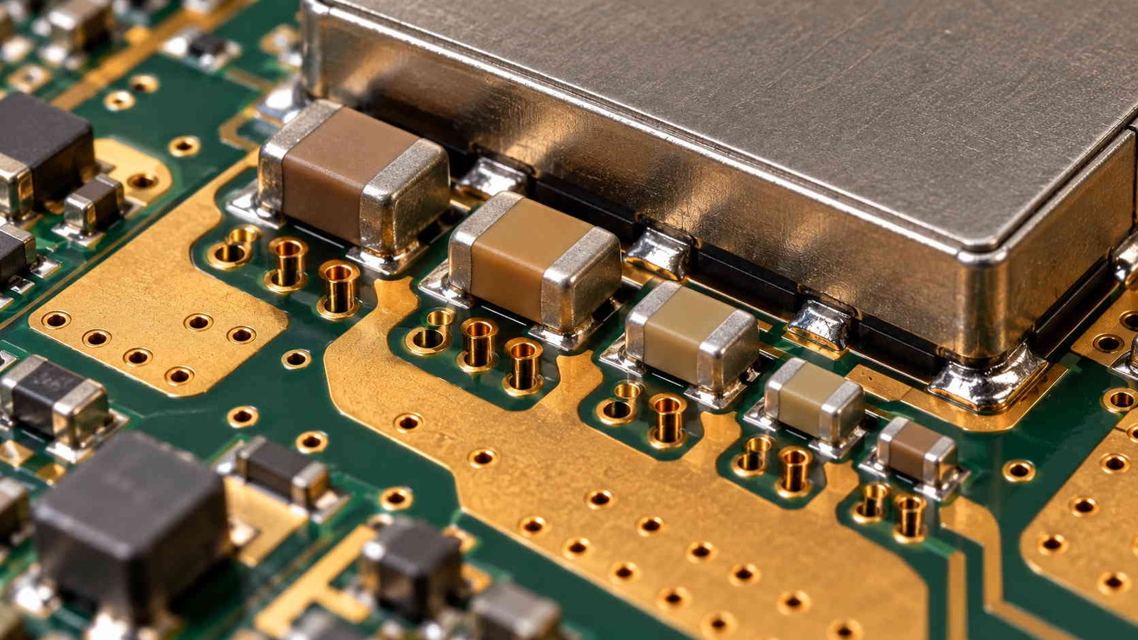
Placement then follows from the loop, not from a rule of thumb about distance. In one microsecond light travels 300 m, so propagation is irrelevant; what matters is that the loop from capacitor to device and back has low inductance, because the capacitor's own ESL is in series with the charge it delivers. That is why several small capacitors outperform one large one at these edge rates, and why via count under the capacitor pads matters more than how far the capacitor is from the device. The general treatment is in our heavy copper high-frequency PCB guide.
3. Inductance Is Cheap Here — But Not Irrelevant
The inductance calculation is worth doing because the answer is generous, and knowing that changes where the engineering effort goes.
| Edge duration | di/dt | Voltage across 1 nH | Voltage across 2 nH | Verdict against a 1 V allowance |
|---|---|---|---|---|
| 100 ns | 3.20e+07 A/s | 32 mV | 64 mV | Comfortable |
| 50 ns | 6.40e+07 A/s | 64 mV | 128 mV | Comfortable |
| 20 ns | 1.60e+08 A/s | 160 mV | 320 mV | 20–32% of the allowance — noticeable, not fatal |
Inductance is not the dominant term at micro-sleep timescales. The loop-area work still matters, but it matters for the switching edges rather than for the sleep duration.
| Target | Value | Derived from | Practical interpretation |
|---|---|---|---|
| Allowed droop | 1 V (2% of 50 V) | A declared design choice | Tighter is possible; it costs capacitance |
| Target impedance, 100 mV goal | 0.031 Ω | 0.1 V ÷ 3.20 A | A very low bar to hit with a decent plane pair |
| Target impedance, 1 V goal | 0.312 Ω | 1 V ÷ 3.20 A | Comfortably met by any solid plane |
| Inductance budget at a 20 ns edge | 6.25 nH | 1 V ÷ 1.60e+08 A/s | Six nanohenries is a lot of loop — the layout is not the constraint here |
The conclusion is uncomfortable for anyone who has spent a career chasing nanohenries: on a DTX timescale, the board's job is to hold charge, not to be fast.
A budget of 6.25 nH is not a difficult layout. It is roughly the loop of a plane pair with a few millimetres of separation and a via field. So the board does not need to be heroic about power integrity — it needs to be correct about it, and then spend its effort on the two things that are actually difficult: keeping the RF reference continuous while carrying 3.2 A, and getting the heat out.
4. Envelope Tracking Is a Second, Different Supply
Envelope tracking raises the drain voltage in step with the signal envelope, so the amplifier is never operating at a back-off it does not need. Electrically it is a second supply with its own bandwidth requirement — roughly the envelope bandwidth, which for a wideband 5G carrier is hundreds of kilohertz to a few megahertz — and its own output impedance target.
The mistake is to fold it into the DC decoupling discussion. The DC bands in the previous section describe a supply that must hold a constant voltage while the load pulses; the tracker describes a supply that must deliberately vary its voltage at signal rate. Their impedance targets live in overlapping frequency ranges but their control objectives are opposite, and a board that treats them as one network ends up with a tracker that cannot move fast enough because it is loaded by too much capacitance, and a DC rail that dips because its capacitance went into the tracker's output.
The board's contribution to the tracker is the connection between its output and the device's drain — short, wide, and with a defined return. That is a different geometry from a decoupling bank, and it is usually the part of the layout that gets copied from a previous design without re-checking, because it looks like a power trace. It is not: at envelope rates it is a transmission path with an impedance that has to stay low across a decade of frequency.
5. The Copper the RF and the DC Both Want
A PA board is the place where the RF and power disciplines stop being separable, because they are asking for the same copper and disagreeing about how thick it should be.
| Shared resource | What the RF path needs | What the DC path needs | Conflict |
|---|---|---|---|
| Ground plane | Continuous reference under every RF line | Low-impedance return for 3.2 A transients | Both want the same copper, and neither tolerates a slot |
| Copper weight | Thin, for fine line definition | Thick, for IR drop and spreading | Resolved by layer: thin RF layers, heavy DC layers |
| Thermal path | Not an RF parameter | Primary design constraint | The DC plane is usually also the heat spreader |
| Enclosure | Defines the cavity and the lid height | Defines the thermal interface | One mechanical decision, two electrical consequences |
A PA board is where the RF and power disciplines stop being separable, because they are competing for the same copper on the same layer.
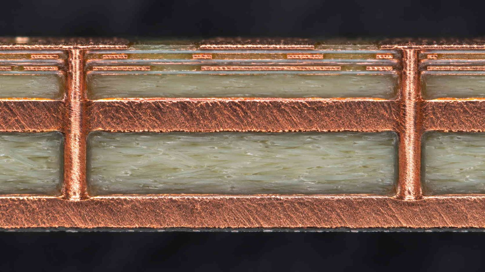
The resolution is layer assignment, and it has to be made before the stackup is frozen. Thin high-frequency layers carry the RF; heavy layers carry the current and spread the heat; via fields join them at defined points rather than wherever a pour happened to end. A board that tries to do both on one layer ends up with either an etch problem in the RF section or an IR-drop problem in the DC section, and usually both.
The hybrid stackup question is worked through in our FR4 and high-frequency hybrid guide, and the copper-weight consequences in the copper thickness and line width guide. What is specific to a DTX board is that the return current is pulsed at 3.2 A, so the ground plane is carrying a spectrum that reaches into the megahertz — right through the band where the RF section is most sensitive to a shared impedance.
6. The Wideband Monitor in the Same Box
Modern base station platforms pair the transmitter with a wideband observation receiver — the class of design that monitors across several Nyquist zones to roughly 18 GHz and extracts narrowband channels digitally. At 18 GHz a free-space wavelength is 16.66 mm, so the monitor's front end and the PA's output network are both compact enough that a shared enclosure makes them neighbours rather than separate systems.
The coupling paths between them are the ground plane and the supply, which is exactly what the previous two sections have been about. A partition drawn on a silkscreen is not a partition; what separates two sections is a continuous ground reference with a defined return, and a supply that does not share an impedance between them. The mixed-signal conventions for that are in our mixed-signal and high-speed RF board design guide and the RF and digital mixed-signal stackup guide.
The monitoring path also has its own first-order requirement, which is phase noise and clock cleanliness rather than current. That is a clock-distribution problem, treated in our RF clock distribution and phase matching guide — and it is the requirement most likely to be damaged by a power section designed solely around the PA.
7. The 5G PA Board RFQ Checklist
Related reading
- 60 GHz dual-beam communication module PCB — element pitch, beam-to-beam isolation and the 57–70 GHz loss budget
- 77 GHz radar SoC PCB design for 4T4R — virtual-array pitch, the phase budget in degrees per millimetre, and Dk batch tolerance
- RF power amplifier PCB design — matching, stability and thermal path
- massive MIMO base-station PCB — steady-state thermal and signal integrity on a dense channel count
Eight lines. The second one changes the bill of materials; the fifth changes the stackup.
| # | Item to specify | Why it decides the outcome |
|---|---|---|
| 1 | Output power, efficiency and the supply rail | Sets the current, and every other number follows |
| 2 | DTX duty cycle and micro-sleep duration | Sets the charge account: 1 µs → 3.2 µF per volt of droop |
| 3 | Edge rate of the PA enable and bias | Sets the inductance requirement, which is generous at 20 ns |
| 4 | Envelope tracking architecture, if used | Adds a supply that must follow the envelope, not the average |
| 5 | Layer assignment: RF, DC, thermal | The only way to resolve the copper-weight conflict |
| 6 | Ground-return continuity under the RF lines | An RF requirement that a power pour can quietly break |
| 7 | Thermal interface and lid | Bulk of the heat leaves through the top, not the board |
| 8 | Evidence package | IR drop, plane impedance, cross-section, thermal imaging |
Eight lines. The second is the one that changes the decoupling bill of materials, and it is the one most often left as 'DTX supported'.
The pattern: a DTX-capable PA board is specified by its charge account and its layer assignment, and proved by IR drop and plane impedance rather than by a functional test. The 36% saving is real, and the board's job is to make sure it arrives without a spectral cost.
5G PA Board Power Integrity — Frequently Asked Questions
DTX charge arithmetic, why inductance is not the limit at 20 ns, envelope tracking versus DC decoupling, and the copper-weight conflict between the RF and DC sections.
Does DTX really need special board design?
It needs a different emphasis rather than a different board. A micro-sleep that removes 3.2 A for a microsecond is a charge event: 3.20 µC has to come from capacitance within the loop, because no regulator responds that fast. Converted to a droop allowance, that is 3.20 µF per volt. Once the capacitance is there and the loop is short, the rest of the design is ordinary power integrity — the point is to size the capacitance from the sleep length rather than by habit.
Is loop inductance the limiting factor for a 20 ns transition?
No, and the arithmetic is worth doing before adding copper. A 3.20 A transition in 20 ns is 1.60e+08 A/s; across 1 nH that is 160 mV, and across 2 nH it is 320 mV — against an allowance of about 1 V. The inductance budget is 6.25 nH, which is generous. Loop area still matters for radiated coupling and for the edges themselves, but it is not what limits a DTX-capable board.
How does envelope tracking change the decoupling requirement?
It adds a supply that has to track the envelope rather than supply an average. That means the tracker's output impedance has to be low over the envelope bandwidth — hundreds of kilohertz to a few megahertz in practice — and the board's contribution is the connection between the tracker and the device. The DC decoupling bands described above do not cover it, and treating the two as one problem produces a board that is good at neither.
Why can't the RF and DC sections use the same copper?
They can, and usually must — but not at the same weight. The RF section needs thin copper for fine line definition and controlled impedance; the DC section needs heavy copper for IR drop and heat spreading at 3.20 A. The resolution is layer assignment: thin high-frequency layers, heavy DC layers, joined by via fields that are designed rather than incidental. Getting this wrong is the most common cause of a PA board that measures well cold and drifts under load.
What does the ground plane have to do with the 36% energy saving?
Nothing directly — the saving comes from not transmitting when there is nothing to transmit. But the mechanism that captures it is a fast, clean bias transition, and that lives on the ground plane. If the return path under the RF lines shares a slot with the DC return, the transient couples into the RF section and the efficiency gain arrives with a spectral regrowth problem attached. The RF reference and the power return are the same copper, and that is the whole design tension.
Isn't an 18 GHz monitoring receiver a separate board?
Usually it is, and it should be, because the requirements diverge: the monitor path wants low loss and low phase noise, the PA path wants current and heat. Where they share an enclosure, the coupling is through the ground plane and the supply, so the two sections need a defined partition rather than a drawn line. The mixed-signal partitioning conventions are in our mixed-signal RF board design guide. At 18 GHz the free-space wavelength is 16.66 mm, so a partition is a real electromagnetic structure, not a silkscreen box.
Designing a 5G PA board that has to survive DTX?
Send the output power, the supply rail, the micro-sleep duration and — if you use it — the envelope tracking architecture. We will size the capacitance from the charge account, set the layer assignment for the RF and DC conflict, define the ground partition, and ship the evidence package — IR drop analysis, plane impedance, cross-section and thermal imaging — with the boards to IPC Class 3.
Contact Us → WhatsApp: +86 137 6047 3650Request a PCB Quote
Upload your Gerber ZIP file and project requirements. Our engineering team will review your PCB material, stackup, impedance needs, surface finish, and production quantity before quoting.
Please prepare:
- Gerber files in ZIP format
- PCB material or stackup requirements
- Controlled impedance notes if available
- Prototype or batch production quantity