
Gap Waveguide PCB: Building an Air Line Out of Vias
D-band gap waveguide PCB design: pin height is your board thickness, the stopband is always 2:1, and a 117 µm lid gap, not the etch, sets 50 Ω at 170 GHz.
Home » 140 GHz PCB » Gap Waveguide PCB: Building an Air Line Out of Vias
Table of Contents
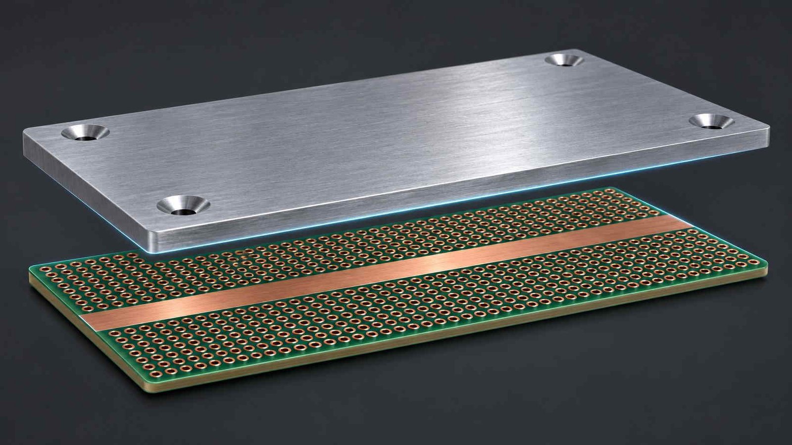
A gap waveguide is what you get when you stop trying to keep the field inside the laminate. Two metal surfaces face each other across an air gap, and one of them is covered in a bed of small pins. The pins make that surface behave as a magnetic wall over a band of frequencies, which stops the parallel-plate mode from propagating — and that single property is what lets the two surfaces be screwed together without touching.
For a board shop the consequence is unusual. In every other high-frequency topology the laminate is in the signal path and its loss tangent is in the budget. Here the laminate is a spacer that holds a few thousand plated holes at a fixed pitch, and the electrical dimensions move to the board thickness and the air gap above it. This page works through that shift: how pin height picks the band, where the loss goes instead, and why the tolerance that decides the impedance is not on the Gerber.
1. Why Put the Field in the Air
At 140 GHz, a millimetre of air between two metal surfaces is a waveguide with no cutoff frequency. Put a microstrip board inside a milled housing and the housing stops being a box and becomes a cavity: energy leaks sideways into plate modes, and the result shows up in S21 as a comb of resonances that shifts when you tighten a screw. Most millimetre-wave packaging problems are a version of this one.
| Topology | Where the field sits | Dominant loss term | Is the laminate's Df in the budget? | Holes required | Lid contact | What sets 50 Ω |
|---|---|---|---|---|---|---|
| Microstrip | In the dielectric | Dielectric + copper | Yes — directly | None (vias for ground) | No lid; mask over the line | Line width and dielectric thickness |
| Substrate-integrated waveguide | In the dielectric | Dielectric + copper | Yes — the field is in the laminate | Two rows of via walls | Contact at the launch and the lid | Waveguide width |
| Ridge gap waveguide | In the air gap | Copper only | Only in the feed layer | Full pin bed, 0.353 mm pitch | No — the pin bed seals without contact | Ridge width and the air gap |
The third row is the only one where the impedance is set by a mechanical gap rather than by the laminate. That is the whole reason the topology exists, and it is also the whole reason it is hard to buy: the critical dimension is not printed.
The three topologies answer it in three different ways, and only the third takes the dielectric out of the loss path. A substrate-integrated waveguide fences the field with via walls: it works, it is well understood, and the field is still in the laminate, so the material's loss tangent stays in your budget. A gap waveguide instead makes the surface itself reflective to plate modes, which is why the lid does not have to be bonded, gasketed, or even in contact.
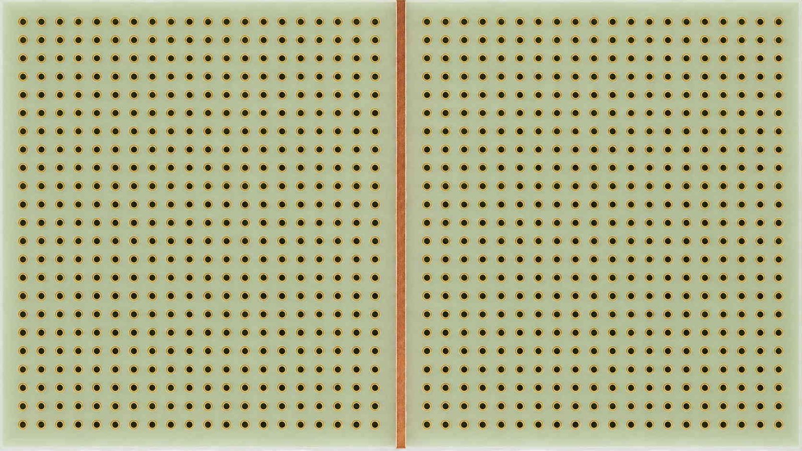
What that changes on the shop floor is the specification for the laminate in the pin layer. It is no longer "low Df, tight Dk"; it is "0.762 mm ±25 µm, flat, 3216 holes at 0.353 mm pitch, no wicking". Those are dimensional requirements, and dimensional requirements are the ones that can be held to a number and audited. What the same band does to a conventional microstrip board is a separate problem, set out in our D-band PCB guide.
2. Pin Height Is a Board Thickness
The pin height is not a free parameter. A pin surface presents a high impedance where the pin is a quarter wave tall and returns to a conductor at a half wave, so the stopband runs from c/4h to c/2h. That is a 2:1 window, always, regardless of what the pins are made of.
| Band (GHz) | λ0 at the low edge | Pin height required | Standard board thickness | Resulting stopband | Pin pitch (≤ λ/5) | Drill | Holes per 400 mm² |
|---|---|---|---|---|---|---|---|
| 57–71 | 5.26 mm | 1.315 mm | 1.524 mm (60 mil) | 49.2–98.4 GHz | 0.844 mm | 0.25 mm | 561 |
| 71–86 | 4.22 mm | 1.056 mm | 1.270 mm (50 mil) | 59.0–118.0 GHz | 0.697 mm | 0.25 mm | 823 |
| 110–170 | 2.73 mm | 0.681 mm | 0.762 mm (30 mil) | 98.4–196.7 GHz | 0.353 mm | 0.20 mm | 3,216 |
| 220–330 | 1.36 mm | 0.341 mm | 0.381 mm (15 mil) | 196.7–393.4 GHz | 0.182 mm | 0.10 mm | 12,117 |
Column three is a calculation; column four is a catalogue. The board thickness you order is the pin height you get, and the stopband follows from it — 0.762 mm lands on 98.4–196.7 GHz, which covers 110–170 GHz with margin at both ends. A 0.508 mm board would start the stopband at 147 GHz and be unusable below it.
Read column three against column four: the pin height you need is a board thickness you can order. 0.762 mm puts the stopband on 98.4–196.7 GHz, which covers 110–170 with margin at both ends. A 0.508 mm board would put it at 147–295 GHz — excellent for the top of the band and useless below 147. This also explains something that looks like an architectural fashion in D-band front-ends: they arrive as band-split modules because no single pin height spans 57 to 170 GHz, a 2.98:1 span asked of a surface that only offers 2:1.
The cost curve is in the last column. Hole count goes as one over pitch squared, so moving from D band to G band multiplies the drilling by 3.8 for the same board area while the aspect ratio barely moves from 3.8:1. You are not buying a harder drill, you are buying twelve thousand holes. Where that stops being sensible is covered in our drilling capability page.
3. Where the Loss Goes Instead
With the field in air, the dielectric term goes to zero and the question becomes what is left.
| Line | Dk / Df at 140 GHz | Dielectric loss | Over 50 mm | What it means |
|---|---|---|---|---|
| PTFE-class laminate | 2.20 / 0.0009 | 0.0200 dB/mm | 1.00 dB | The best a filled laminate does at this band |
| Mid-loss hydrocarbon | 3.00 / 0.0025 | 0.0676 dB/mm | 3.38 dB | 3.4× the loss above, same geometry |
| Air line (ridge gap) | 1.00 / 0.000 | 0 dB/mm | 0 dB | Dielectric term removed; copper remains on ridge and lid |
Conductor loss does not disappear: at 140 GHz the skin depth is 0.174 µm and the surface resistance 0.096 Ω/sq, so surface finish still matters — but on two flat surfaces instead of a 0.127 mm dielectric.
One decibel per 50 mm is the best a filled laminate does at 140 GHz, and a mid-loss material costs 3.4 times that. In a gap waveguide that term leaves the line, and what remains is conductor loss on the ridge and the lid: at 140 GHz a skin depth of 0.174 µm and a surface resistance of 0.096 Ω/sq. Same physics that makes surface finish matter on any millimetre-wave board — applied to two flat surfaces instead of a 0.127 mm dielectric.
That is a topology comparison and nothing more. It does not make the laminate unnecessary: a D-band module normally has a feed network on one layer that does want a low-loss material, and a pin layer whose requirement is dimensional. Two different specification sheets inside one stackup is the normal outcome, not a compromise. The material behaviour behind both is described in our Dk and Df performance page.
4. The 50 Ω Nobody Draws
A ridge gap waveguide is a metal ridge running between two rows of pins, with the lid above it. Treat the ridge-to-lid region as a parallel plate and 50 Ω collapses to a single relation: the ridge width is 7.53 times the air gap. Wide ridge, wide gap; narrow ridge, narrow gap.
| Air gap | Ridge width for 50 Ω | Transverse resonance limit | Usable at 110–170 GHz? |
|---|---|---|---|
| 0.100 mm | 0.753 mm | 198.9 GHz | Yes — margin to 199 GHz |
| 0.117 mm | 0.882 mm | 170.0 GHz | Marginal — lands exactly on 170 GHz |
| 0.150 mm | 1.130 mm | 132.6 GHz | No — fails above 133 GHz |
| 0.200 mm | 1.507 mm | 99.5 GHz | No — fails above 99 GHz |
A parallel plate radiates sideways once the ridge reaches λ0/2, so the ridge width is capped at 0.882 mm at 170 GHz. Working backwards through 50 Ω = 377·g/w, that caps the air gap at 0.117 mm. The gap, not the etch, is the dimension that decides the geometry at the top of D band.
The third column is the constraint that actually decides the geometry, and it is the one that gets missed. A parallel plate radiates sideways once the ridge reaches a half wavelength, and at 170 GHz that is 0.882 mm. So the ridge cannot be widened to suit a comfortable 0.2 mm gap: 0.2 mm would demand a 1.51 mm ridge, which is overmoded above 99 GHz. Working backwards, 170 GHz permits a gap of 0.117 mm — a mechanical feature about a tenth of a millimetre tall, set by lid standoff and board thickness, and written nowhere on the fabrication drawing. In this topology, impedance control is a stack-up and machining question before it is an etch question; the etch side of it is covered under controlled impedance.
5. Tolerance Lives in the Assembly
The table below is worth taking to a design review, because it puts the fabrication tolerance and the assembly tolerance into the same unit.
| Tolerance | Nominal | Impedance effect | Return loss | Where it comes from |
|---|---|---|---|---|
| Ridge width ±0.020 mm | 0.882 mm | 2.27% | −38.9 dB | Etch and plating |
| Air gap ±0.025 mm | 0.117 mm | 21.4% | −19.4 dB | Lid standoff, board thickness, flatness |
| Pin height ±0.025 mm | 0.762 mm | stopband edge ±3.28% | — | Laminate thickness tolerance |
| Pin position ±0.025 mm | copper web 0.1527 mm | 16.4% of the web | — | Drill registration |
| Lid contact | none required | — | — | 3 rows of pins = 1.06 mm seal |
The first two rows are the argument of this page. Etching 20 µm off the ridge is a −39 dB return loss; closing the lid 25 µm too far is −19 dB. The assembly is 9.4× more sensitive than the copper, and only the copper appears on a PCB purchase order.
Etching the ridge 20 µm wide of nominal is a 2.3% impedance error — a −39 dB return loss, irrelevant next to anything else in the chain. Moving the lid 25 µm closer is a 21% error and −19 dB, which dominates everything the board shop spent money on. The two differ by 9.4 times, and only one of them appears on a purchase order for a PCB.
The compensation runs the other way from what people expect. Because the pin bed blocks plate-mode leakage, the lid needs no electrical contact: three rows of pins, 1.06 mm of width, seal the perimeter, and the lid can be a flat plate on four screws instead of a milled, gasketed, torqued assembly. That is a genuinely relaxed requirement — but relaxed in the contact dimension, not the spacing dimension. You no longer have to guarantee that two metals touch. You still have to know the gap to 25 µm.
One geometric consequence is worth flagging early. At 140 GHz a quarter-wave section in air is 0.535 mm, which is shorter than the 0.762 mm board is thick — by a factor of 1.42. A transition that runs vertically through the board therefore cannot be a quarter-wave transformer at this frequency; it has to be a lateral structure on the top surface with the pin bed carried around it. Transitions of that kind, including the ones between a planar line and a hollow guide, are treated in our PCB to waveguide transition guide.
6. The DFM Checklist, and Where This Stops Working
Related reading
- D-band PCB design — loss budget, thin cores and via practice from 110 to 170 GHz
- PCB to waveguide transition design — the launch geometry and its alignment tolerance
- 110–145 GHz calibration board — reference planes above 100 GHz
- X- and Ku-band AESA radar PCB — T/R channel density, cooling and lot consistency from 8 to 18 GHz
Eight lines, in the order they decide the outcome.
| # | Item to specify | Why it decides the outcome |
|---|---|---|
| 1 | The stopband, not the application band | The pin surface does not know what you are building; a 2:1 window is all it offers |
| 2 | Board thickness as an electrical dimension, with tolerance | It is the pin height: ±25 µm moves the stopband edge ±3.3% |
| 3 | Drill and pitch together, plus the copper web | 0.20 mm drill on 0.353 mm pitch leaves 0.1527 mm of web — state both |
| 4 | How many pin rows around the ridge, and where the bed stops | Two rows is a fence, three rows is a seal; the transition needs a corridor |
| 5 | Ridge width and air gap as one number pair | 50 Ω is two dimensions, and only one of them is on the Gerber |
| 6 | Flatness of the face that closes the gap | The gap has no contact tolerance to absorb a warp |
| 7 | Which side the transition lands on | A quarter wave in air is 0.535 mm, shorter than the 0.762 mm board is thick |
| 8 | Hole count per panel, not board area | 3216 holes at D band, 12116 at G band for the same 400 mm² |
Line 5 is the one that gets lost in a drawing package: the etch is specified to ±20 µm and the gap is left to the mechanical assembly, where it is good to ±50 µm and nobody converts it to ohms.
Two of these are usually missing from a first drawing package, and both are cheap to fix at review rather than at build: the stopband (line 1) and the gap (line 5). A quote that starts from "which laminate" and never reaches "which gap" is answering the wrong question.
The last row is the business case rather than the electrical one. A 400 mm² board at D band carries 3216 plated holes; the same board at G band carries 12116. Above roughly 200 GHz the pitch drops below 0.2 mm and the drill below 0.1 mm, and at that point a machined pin bed in metal holds tolerance better than any laminate — so the PCB's honest role becomes the feed layer, with the pin bed handed to a machinist. Knowing where that line falls, rather than quoting past it, is most of what a D-band supplier conversation should consist of. The review process behind these checks is described in our DFM review guide, and the batch evidence a customer can audit in our RF PCB quality control guide.
Gap Waveguide PCB — Frequently Asked Questions
Why the pin height is a board thickness, why the stopband is always 2:1, and why the air gap — not the etch — is the number that decides whether the module works.
What is a gap waveguide, in one paragraph?
Two metal surfaces facing each other across an air gap, one of which is covered in a bed of small pins. The pins make that surface behave as a magnetic wall over a band of frequencies, which stops the parallel-plate mode from propagating between the plates. Because that mode is what normally forces a housing to be a sealed, contacted cavity, suppressing it lets the two surfaces be screwed together without touching — and it lets the transmission line itself run in air rather than in laminate.
Why is the stopband always 2:1?
Because it is bracketed by two boundary conditions rather than by a design choice. A pin surface is high-impedance where the pin is a quarter wavelength and returns to a conductor at a half wavelength, so the useful window runs from c/4h to c/2h. That ratio is 2 whatever the pins are made of. It is why 110–170 GHz (1.55:1) fits comfortably on one board and 57–170 GHz (2.98:1) cannot, and why D-band front-ends arrive as band-split modules.
Can the pin layer be built on an ordinary laminate?
The pin layer is not selected for loss, because the field is not in it — it is selected for thickness tolerance, flatness and dimensional stability under assembly. That is a different question from 'which laminate is lowest loss', and the two answers do not have to be the same material. Most D-band modules end up with a low-loss feed layer and a dimensionally stable pin layer, which is a hybrid stackup rather than a compromise. Our hybrid stackup page covers how the two are laminated together.
Why does the lid not have to touch?
Because the pin bed already blocks the mode that would leak. A contacted lid is the traditional way to stop plate-mode leakage, and it costs you a milled, gasketed, torqued assembly with a flatness requirement on both faces. With a pin bed, three rows — 1.06 mm of width — seal the perimeter and the lid can be a flat plate on four screws. What is relaxed is the contact requirement. What is not relaxed is the spacing: the gap still has to be known to 25 µm.
How tight does the air gap really have to be?
At 170 GHz, 50 Ω on a ridge narrower than 0.882 mm needs a 0.117 mm gap. A ±25 µm assembly error on that is a 21.4% impedance error and a −19.4 dB return loss, against −38.9 dB for ±20 µm of etch error — 9.4× more sensitive. Practically: the gap is set by lid standoff and board thickness, so both have to be called out, and the mating face has to be flat enough that the gap does not vary across the board.
Do the pin vias have the stub problem that signal vias do?
No, and that is a useful inversion. A pin is a full-thickness plated hole that terminates at the pad on the far side: there is no unused length hanging below the plane, so no stub resonance to back-drill. The signal vias that carry the feed into and out of the pin-bed region are a different matter — they are ordinary mmWave signal vias with all the usual stub and return-path problems, covered in our RF via design guide.
Building a pin bed for D band?
Send the stopband you need, the board outline and how the lid closes. We will pick the thickness that puts the stopband where you want it, check the pitch and copper web against our drilling capability, and quote the hole count honestly — including the case where a machined pin bed is the better answer.
Contact Us → WhatsApp: +86 137 6047 3650Request a PCB Quote
Upload your Gerber ZIP file and project requirements. Our engineering team will review your PCB material, stackup, impedance needs, surface finish, and production quantity before quoting.
Please prepare:
- Gerber files in ZIP format
- PCB material or stackup requirements
- Controlled impedance notes if available
- Prototype or batch production quantity